SST89V516RD2-33-C-TQI View Datasheet(PDF) - Silicon Storage Technology
Part Name
Description
View to exact match
SST89V516RD2-33-C-TQI Datasheet PDF : 81 Pages
| |||
Data Sheet
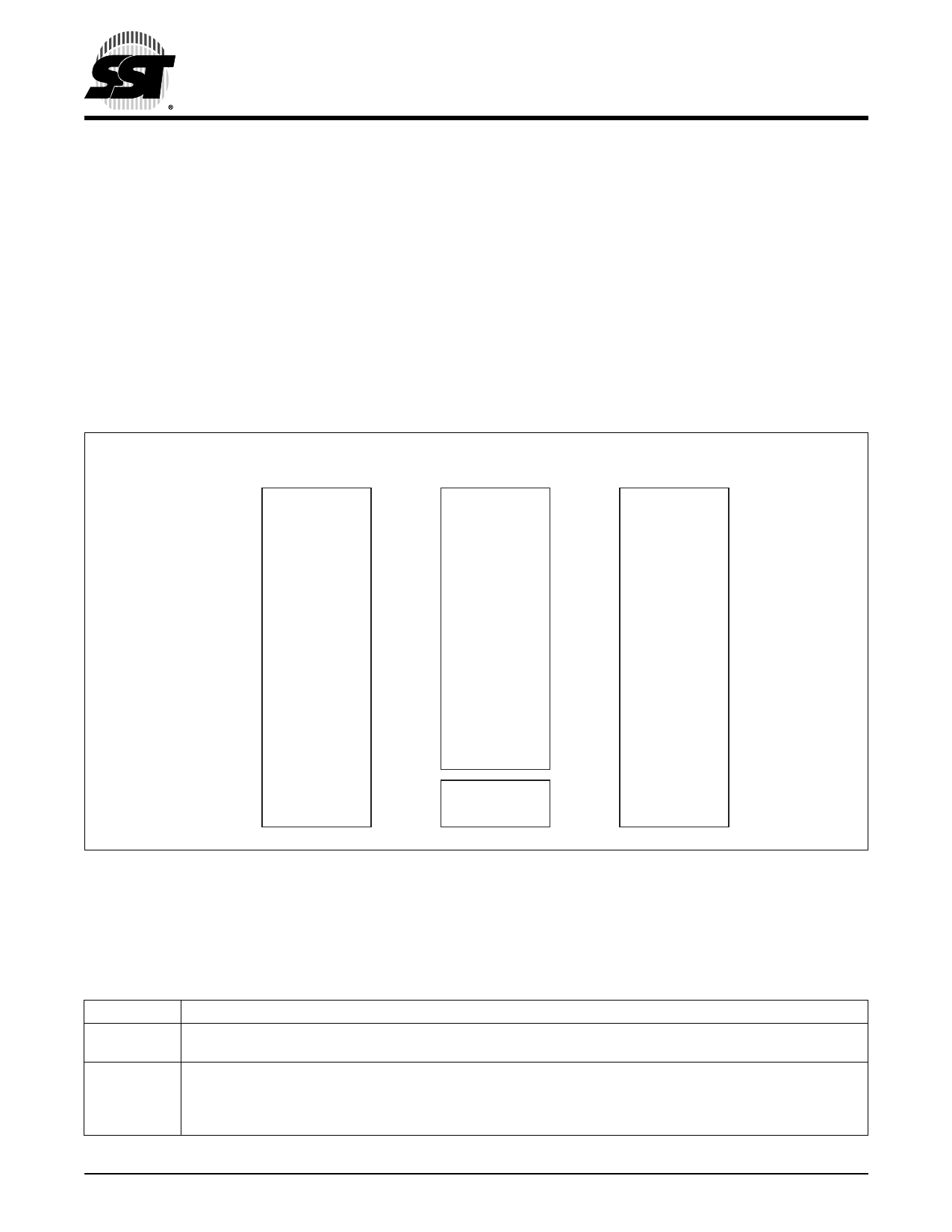
3.0 MEMORY ORGANIZATION
The device has separate address spaces for program and
data memory.
3.1 Program Flash Memory
There are two internal flash memory blocks in the device.
The primary flash memory block (Block 0) has 64 KByte.
The secondary flash memory block (Block 1) has 8 KByte.
Since the total program address space is limited to 64
KByte, the SFCF[1:0] bit are used to control program bank
FlashFlex MCU
SST89E516RD2 / SST89E516RD
SST89V516RD2 / SST89V516RD
selection. Please refer to Figure 3-1 for the program mem-
ory configuration. Program bank selection is described in
the next section.
The 64K x8 primary SuperFlash block is organized as 512
sectors, each sector consists of 128 Bytes.
The 8K x8 secondary SuperFlash block is organized as 64
sectors, each sector consists also of 128 Bytes.
For both blocks, the 7 least significant program address bits
select the byte within the sector. The remainder of the pro-
gram address bits select the sector within the block.
FFFFH
EA# = 0
EA# = 1
SFCF[1:0] = 00
FFFFH
EA# = 1
SFCF[1:0] = 01, 10, 11
FFFFH
External
64 KByte
56 KByte
Block 0
64 KByte
Block 0
0000H
2000H
1FFFH
0000H
8 KByte
Block 1
FIGURE 3-1: Program Memory Organization
0000H
1273 F01.0
3.2 Program Memory Block Switching
The program memory block switching feature of the device allows either Block 1 or the lowest 8 KByte of Block 0 to be
used for the lowest 8 KByte of the program address space. SFCF[1:0] controls program memory block switching.
TABLE 3-1: SFCF Values for Program Memory Block Switching
SFCF[1:0]
01, 10, 11
00
Program Memory Block Switching
Block 1 is not visible to the program counter (PC).
Block 1 is reachable only via in-application programming from 0000H - 1FFFH.
Block 1 is overlaid onto the low 8K of the program address space; occupying address locations 0000H - 1FFFH.
When the PC falls within 0000H - 1FFFH, the instruction will be fetched from Block 1 instead of Block 0.
Outside of 0000H - 1FFFH, Block 0 is used. Locations 0000H - 1FFFH of Block 0 are reachable through
in-application programming.
T3-1.0 1273
©2007 Silicon Storage Technology, Inc.
12
S71273-03-000
1/07
Share Link: 