SST89E54RD2A View Datasheet(PDF) - Silicon Storage Technology
Part Name
Description
View to exact match
SST89E54RD2A Datasheet PDF : 84 Pages
| |||
FlashFlex MCU
SST89E54RD2A/RDA / SST89E58RD2A/RDA
SST89V54RD2A/RDA / SST89V58RD2A/RDA
Data Sheet
read and write signals (P3.6 - WR# and P3.7 - RD#) for
external memory use. Table 3-3 shows external data mem-
ory RD#, WR# operation with EXTRAM bit.
The stack pointer (SP) can be located anywhere within the
256 bytes of internal RAM (lower 128 bytes and upper 128
bytes). The stack pointer may not be located in any part of
the expanded RAM.
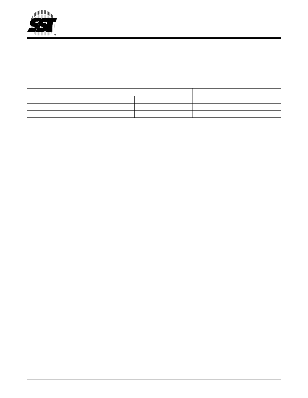
TABLE 3-3: External Data Memory RD#, WR# with EXTRAM bit
MOVX @DPTR, A or MOVX A, @DPTR
AUXR
EXTRAM = 0
EXTRAM = 1
ADDR < 0300H
RD# / WR# not asserted
RD# / WR# asserted
ADDR >= 0300H
RD# / WR# asserted
RD# / WR# asserted
1. Access limited to ERAM address within 0 to 0FFH; cannot access 100H to 02FFH.
MOVX @Ri, A or MOVX A, @Ri
ADDR = Any
RD# / WR# not asserted1
RD# / WR# asserted
T3-3.0 1339
©2007 Silicon Storage Technology, Inc.
16
S71339-01-000
1/07
Share Link: 