SST89E54RDA(2011) View Datasheet(PDF) - Silicon Storage Technology
Part Name
Description
View to exact match
SST89E54RDA Datasheet PDF : 91 Pages
| |||
A Microchip Technology Company
FlashFlex MCU
SST89E54RD2A/RDA / SST89E58RD2A/RDA
Not Recommended for New Designs
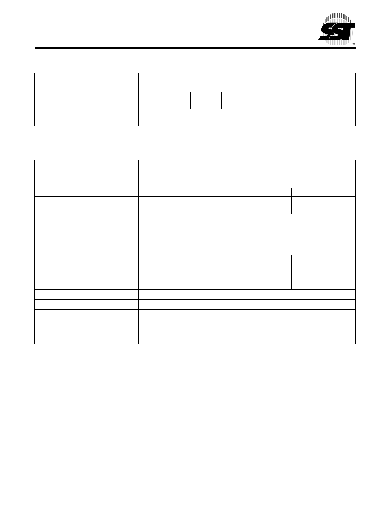
SuperFlash Configuration Register (SFCF)
Location
7
6
5
4
3
2
1
0
Reset Value
B1H
-
IAPEN
-
-
-
-
SWR BSEL x0xxxx00b
Symbol
IAPEN
SWR
BSEL
Function
Enable IAP operation
0: IAP commands are disabled
1: IAP commands are enabled
Software Reset
See Section , “Software Reset”
Program memory block switching bit
See Figures 5 and 6 and Table 3
SuperFlash Command Register (SFCM)
Location
7
6
B2H
FIE
FCM6
5
FCM5
4
FCM4
3
FCM3
2
FCM2
1
FCM1
0
Reset Value
FCM0
00H
Symbol
FIE
FCM[6:0]
Function
Flash Interrupt Enable.
0: INT1# is not reassigned.
1: INT1# is re-assigned to signal IAP operation completion.
External INT1# interrupts are ignored.
Flash operation command
000_0001bChip-Erase
000_1011bSector-Erase
000_1101bBlock-Erase
000_1100bByte-Verify1
000_1110bByte-Program
000_1111bProg-SB1
000_0011bProg-SB2
000_0101bProg-SB3
000_1001bProg-SC0
000_1001bProg-SC1
000_1000bEnable-Clock-Double
All other combinations are not implemented, and reserved for future use.
1. Byte-Verify has a single machine cycle latency and will not generate any INT1# interrupt regardless of
FIE.
SuperFlash Address Registers (SFAL)
Location
7
B3H
6
5
4
3
2
1
SuperFlash Low Order Byte Address Register
0
Reset Value
00H
Symbol
SFAL
Function
Mailbox register for interfacing with flash memory block. (Low order address
register).
©2011 Silicon Storage Technology, Inc.
21
DS25114A
12/11
Share Link: 