UT62L12916-100 View Datasheet(PDF) - Utron Technology Inc
Part Name
Description
View to exact match
UT62L12916-100 Datasheet PDF : 12 Pages
| |||
UTRON
Rev. 1.0
UT62L12916/UT62L12916(I)
128K X 16 BIT LOW POWER CMOS SRAM
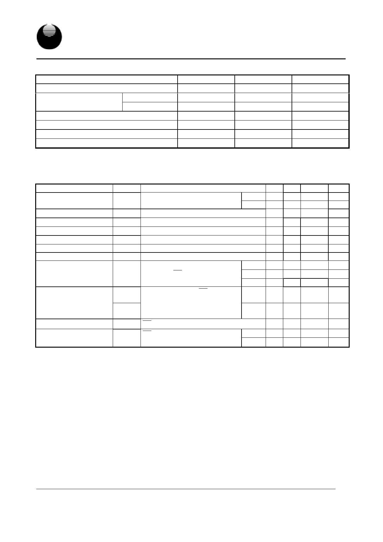
ABSOLUTE MAXIMUM RATINGS*
PARAMETER
SYMBOL
RATING
UNIT
Terminal Voltage with Respect to VSS
VTERM
-0.5 to 4.6
V
Operating Temperature
Commercial
TA
0 to 70
℃
Industrial
TA
-40 to 85
℃
Storage Temperature
TSTG
-65 to 150
℃
Power Dissipation
PD
1
W
DC Output Current
IOUT
50
mA
Soldering Temperature (under 10 secs)
Tsolder
260
℃
*Stresses greater than those listed under “Absolute Maximum Ratings” may cause permanent damage to the device. This is a stress
rating only and functional operation of the device or any other conditions above those indicated in the operational sections of this
specification is not implied. Exposure to the absolute maximum rating conditions for extended period may affect device reliability.
DC ELECTRICAL CHARACTERISTICS (TA = 0℃ to 70℃/-40℃ to 85℃(I))
PARAMETER
SYMBOL TEST CONDITION
MIN. TYP.
Power Voltage
VCC
55
2.7 3.0
70/100 2.5 -
Input High Voltage
Input Low Voltage
Input Leakage Current
Output Leakage Current
Output High Voltage
VIH*1
VIL*2
ILI
ILO
VOH
VSS ≦VIN ≦VCC
VSS ≦VI/O ≦VCC; Output Disable
IOH= -1mA
2.2 -
-0.2 -
-1 -
-1 -
2.2 -
Output Low Voltage
VOL IOL= 2.1mA
--
Operating Power
Supply Current
Cycle time=min, 100%duty
ICC
I/O=0mA, CE =VIL
55 - 30
70 - 25
100 - 20
Average Operation
Current
ICC1
100%duty,II/O=0mA, CE ≦0.2V,
other pins at 0.2V or Vcc-0.2V
Tcycle=
1µs
-
4
ICC2
Tcycle=
500ns
-
8
Standby Current (TTL)
ISB
CE =VIH, other pins =VIL or VIH
- 0.3
Standby Current (CMOS) ISB1
CE =VCC-0.2V
other pins at 0.2V or Vcc-0.2V
-L
- 20
-LL - 2
Notes:
1. Overshoot : Vcc+3.0v for pulse width less than 10ns.
2. Undershoot : Vss-3.0v for pulse width less than 10ns.
3. Overshoot and Undershoot are sampled, not 100% tested.
MAX.
3.6
3.6
VCC+0.3
0.6
1
1
-
0.4
45
35
25
5
10
0.5
80
20
UNIT
V
V
V
V
µA
µA
V
V
mA
mA
mA
mA
mA
mA
µA
µA
UTRON TECHNOLOGY INC.
1F, No. 11, R&D Rd. II, Science-Based Industrial Park, Hsinchu, Taiwan, R. O. C.
TEL: 886-3-5777882 FAX: 886-3-5777919
4
P80042
Share Link: 