SAA4951 View Datasheet(PDF) - Philips Electronics
Part Name
Description
View to exact match
SAA4951 Datasheet PDF : 25 Pages
| |||
Philips Semiconductors
Memory controller
Preliminary specification
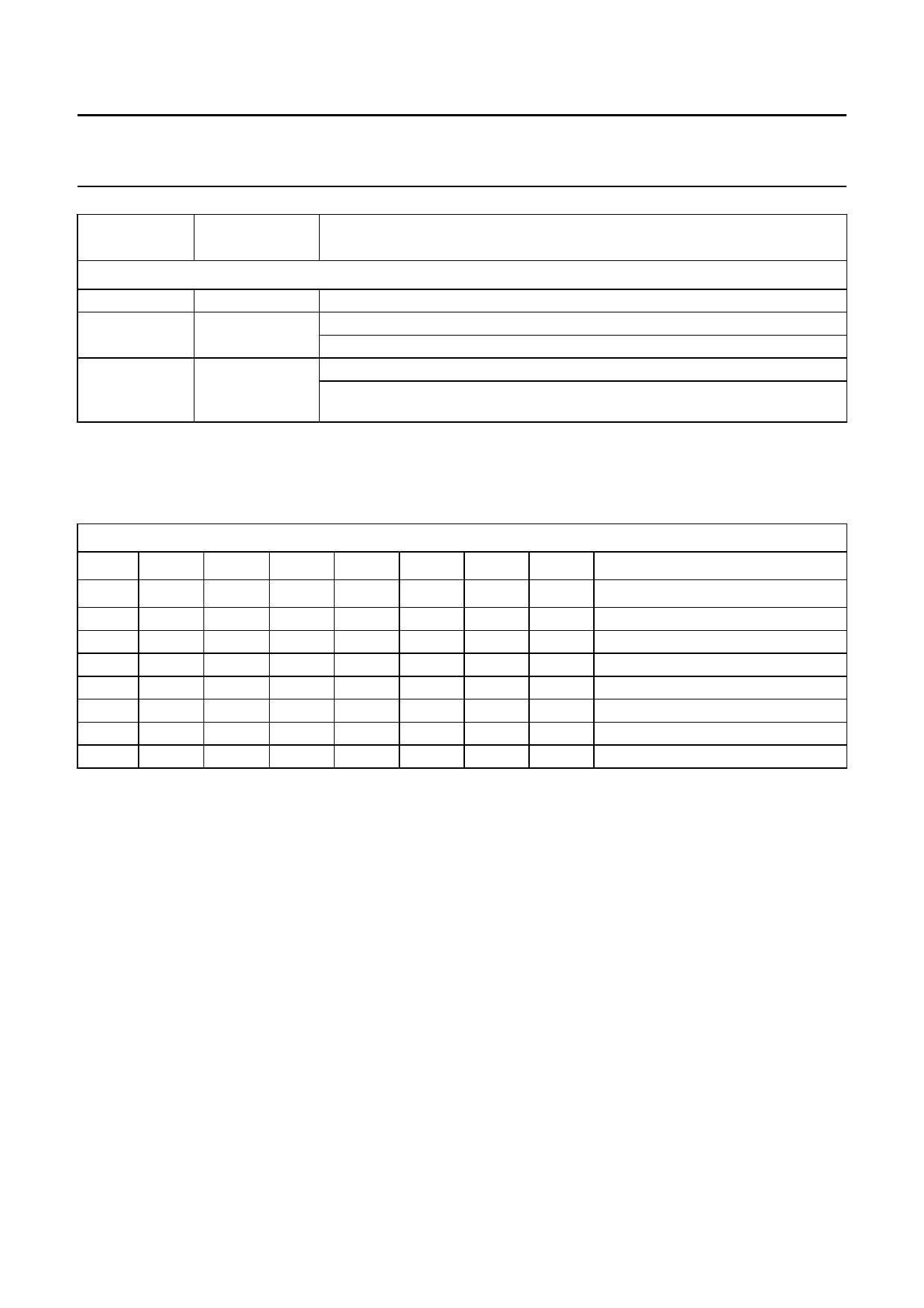
SAA4951
ADDRESS
(HEX)
REGISTER
FUNCTION
Registers to turn on different modes
60
MODE0
61
MODE1
80
READ
mode register 0
mode register 1
the bits of the two mode registers define the operating mode of the SAA4951
read mode
by sending this address the SAA4951 is switched to output mode for the next
address/data cycle, i. e. the microcontroller reads data from the SAA4951
As it can be seen from the above table the registers form groups which are reflected in the addressing scheme according
to Table 2.
Table 2 Internal register addressing scheme.
INTERNAL REGISTER ADDRESS
RW
OP
MO
AD
HV
D2
D1
D0
7
6
5
4
3
2
1
0
1
X
X
X
X
X
X
X
0
0
X
X
X
X
X
X
0
1
1
X
X
X
X
D
0
1
0
1
1
D
D
D
0
1
0
1
0
D
D
D
0
1
0
0
1
D
D
D
0
1
0
0
0
D
D
D
Note
1. X = don’t care, D = data bit
microcontroller reads data
all registers off
select mode 1 / mode 2
select hor. ACQ registers
select vert. ACQ registers
select hor. DSP registers
select vert. DSP registers
bit names:
RW
read/write bit: 1 = read, 0 = write
OP
operate bit, must be 1 to address any register
MO
mode bit, select mode registers
AD
select acquisition (= 1) or display (= 0) registers
HV
select horizontal (= 1) or vertical (= 0) registers
D2
data bit 2
D1
data bit 1
D0
data bit 0
The bits of the two mode registers control the operation modes.
April 1994
10
Share Link: 