GLT6100L08LL-85TC View Datasheet(PDF) - G-Link Technology
Part Name
Description
View to exact match
GLT6100L08LL-85TC Datasheet PDF : 10 Pages
| |||
G-LINK
GLT6100L16
Ultra Low Power 64k x 16 CMOS SRAM
May 2000(Rev. 0.3)
Features :
Description :
∗ Low-power consumption.
The GLT6100L16 is a low power CMOS Static
-Active: 40mA Icc at 55ns.
RAM organized as 65,536 words by 16 bits. Easy
-Stand by :
memory expansion is provided by an active LOW CE
5 µA (CMOS input / output)
1 µA (CMOS input / output, SL)
and OE pin.
∗ Single +2.7 to 3.3V Power Supply.
∗ Equal access and cycle time.
This device has an automatic power – down
mode feature when deselected. Separate Byte
∗ 55/70/85/100 ns access time.
Enable controls ( BLE and BHE ) allow individual
∗ Tri-state output.
bytes to be accessed. BLE controls the lower bits
∗ Automatic power-down when
deselected.
I/O0 – I/O7. BHE controls the upper bits I/O8 – I/O15.
Writing to these devices is performed by taking
∗ Multiple center power and ground pins Chip Enable CE with Write Enable WE and byte
for improved noise immunity.
∗ Individual byte controls for both Read
and Write cycles.
∗ Available in 44pin TSOPII Package.
Enable ( BLE / BHE ) Low.
Reading from the device is performed by taking
Chip Enable CE with Output enable OE and byte
Enable ( BLE / BHE ) Low while Write Enable WE
is held HIGH.
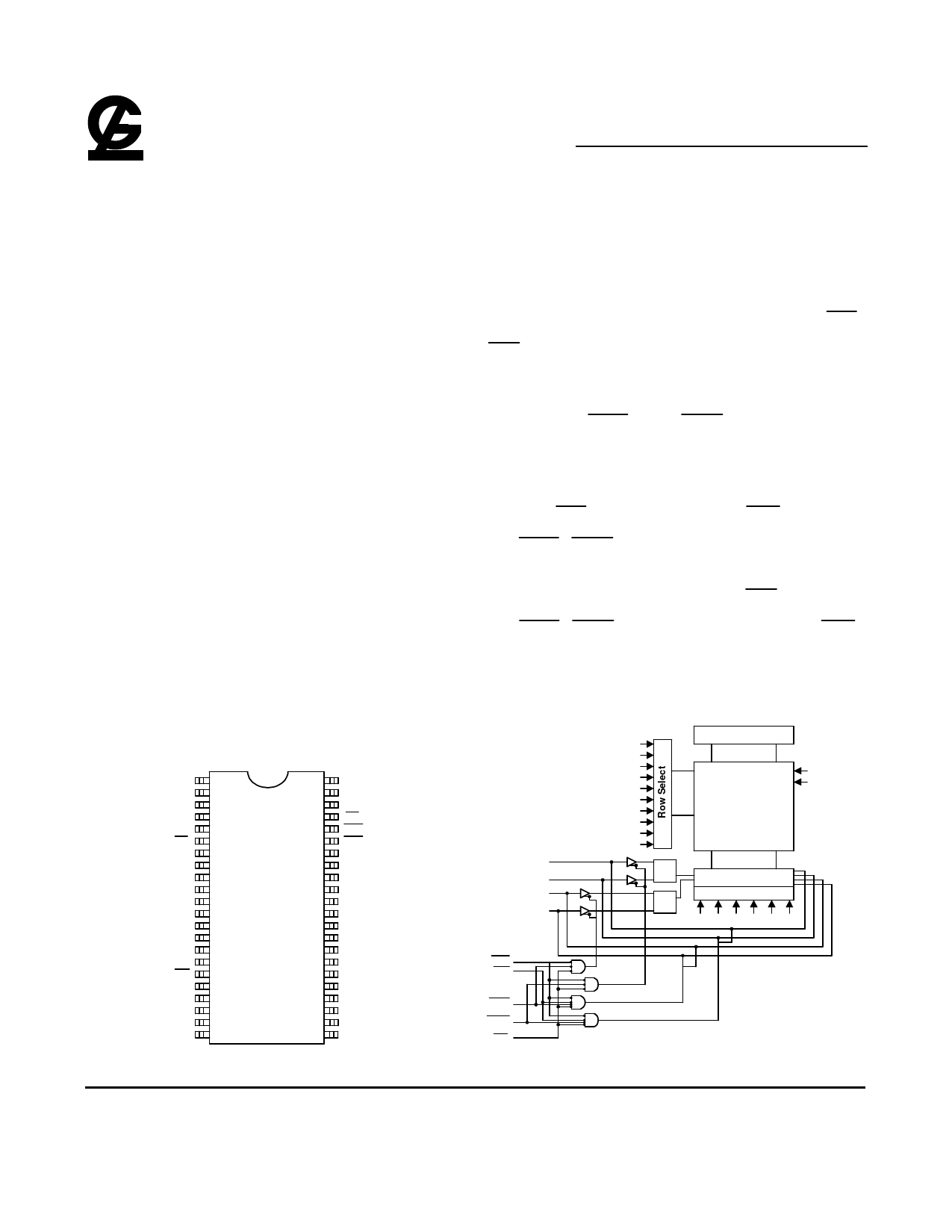
Pin Configurations :
Function Block Diagram :
GLT6100L16
A4
1
A3
2
A2
3
A1
4
A0
5
CE
6
I/O0
7
I/O1
8
I/O2
9
I/O3
10
Vcc 11
Vss 12
I/O4
13
I/O5
14
I/O6
15
I/O7
16
WE 17
A15
18
A14
19
A13
20
A12
21
NC
22
44
A5
43
A6
42
A7
41
OE
40 BHE
39
BLE
38
I/O15
37
I/O14
36
I/O13
35
I/O12
34
Vss
33
Vcc
32
I/O11
31
I/O10
30
I/O9
29
I/O8
28
NC
27
A8
26
A9
25
A10
24
A11
23
NC
I/O0 - I/O7
I/O8 - I/O15
WE
OE
BLE
BHE
CE
Pre-Charge Circuit
A0
A1
A2
Vcc
A3
Vss
A4
Memory Array
A5
A6
A7
1024 x 1024
A8
A9
Data
Circuit
Data
Circuit
I/O Circuit
Column Select
A10 A11 A12 A13 A14 A15
G-Link Technology Corporation
2701 Northwestern Parkway
Santa Clara, CA 95051, U.S.A.
-1-
G-Link Technology Corporation, Taiwan
6F No. 24-2, Industry E. RD. IV, Science Based
Industrial Park, Hsin Chu, Taiwan.
Share Link: 