PT6355-LQ View Datasheet(PDF) - Princeton Technology
Part Name
Description
View to exact match
PT6355-LQ Datasheet PDF : 20 Pages
| |||
PT6355
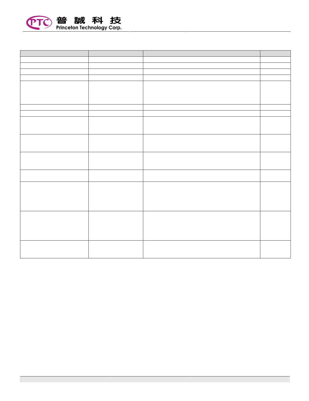
PIN DESCRIPTION
Pin Name
I/O
VCC
-
OSC2
O
VSS
-
OSC1
I
/Reset
I
AN5 to AN0
I
/CS
I
SIN
I
SOUT
O
n-channel open drain
SCLK
I
VEE
-
GR0/P0 to GR7/P7
O
p-channel open drain
GR8/SEG17 to GR17/SEG8
O
p-channel open drain
SEG0 to SEG7
O
p-channel open drain
Description
Power supply
Oscillation output pin
Power supply
Oscillation input pin
Reset input pin
Active ”L”
Internal pull-high resistors are connected between
this pin and the VCC pins.
Analog to digital pin
Chip select
Serial input pin
The clock is read twice with a 2MHz sampling rate
in order to judge if the signal is a noise or not.
Serial output pin
During the Reset condition, this pin is in
high-impedance state.
Serial clock input pin
The clock is read twice with a 2MHz sampling rate
in order to judge if the signal is a noise or not.
Pull-down power supply
Supplies voltage to Pull-down resistors
Grid/Port output pins
This pin acts as either a Grid Output Pin or as an
Ordinary Port Terminal.
During the reset condition, this pin is set to VEE
via a pull-down resistor.
Grid/Segment output pins
This pin acts as either a Grid Output Pin or as an
Segment Output Pin.
During the reset condition, this pin is set to VEE
via a pull-down resistor.
Segment output pin
During the reset condition, this pin is set to VEE
via a pull-down resistor.
Pin No.
1, 44
2
3
4
5
6 to 11
12
13
14
15
16, 17
18 to 25
26 to 35
43 to 36
V1.6
4
Share Link: 