SL74HC251D View Datasheet(PDF) - System Logic Semiconductor
Part Name
Description
View to exact match
SL74HC251D
System Logic Semiconductor

SL74HC251D Datasheet PDF : 5 Pages
| |||
SL74HC251
AC ELECTRICAL CHARACTERISTICS(CL=50pF,Input tr=tf=6.0 ns)
Symbol
Parameter
tPLH, tPHL Maximum Propagation Delay, Input D to
Output Y or Y (Figures 1,2 and 5)
tPLH, tPHL Maximum Propagation Delay , Input A to
Output Y or Y (Figures 3 and 5)
tPLZ, tPHZ Maximum Propagation Delay , Output Enable to
Output Y (Figures 4 and 6)
tPZL, tPZH Maximum Propagation Delay , Output Enable to
Output Y (Figures 4 and 6)
tPLZ, tPHZ Maximum Propagation Delay , Output Enable to
Output Y (Figures 4 and 6)
tPZL, tPZH Maximum Propagation Delay , Output Enable to
Output Y (Figures 4 and 6)
tTLH, tTHL Maximum Output Transition Time, Any Output
(Figures 1 and 6)
CIN
Maximum Input Capacitance
COUT Maximum Three-State Output Capacitance
(Output in High-Impedance State)
VCC
Guaranteed Limit
V 25 °C to ≤85°C ≤125°C Unit
-55°C
2.0 185
230
280
ns
4.5 37
46
56
6.0 31
39
48
2.0 205
255
310
ns
4.5 41
51
62
6.0 35
43
53
2.0 195
245
295
ns
4.5 39
48
59
6.0 33
42
50
2.0 145
180
220
ns
4.5 29
36
44
6.0 25
31
38
2.0 220
275
330
ns
4.5 44
55
66
6.0 37
47
56
2.0 150
190
225
ns
4.5 30
38
45
6.0 26
33
38
2.0 75
95
110
ns
4.5 15
19
22
6.0 13
16
19
-
10
10
10
pF
-
15
15
15
pF
Power Dissipation Capacitance (Per Package)
CPD Used to determine the no-load dynamic power
consumption: PD=CPDVCC2f+ICCVCC
Typical @25°C,VCC=5.0 V
36
pF
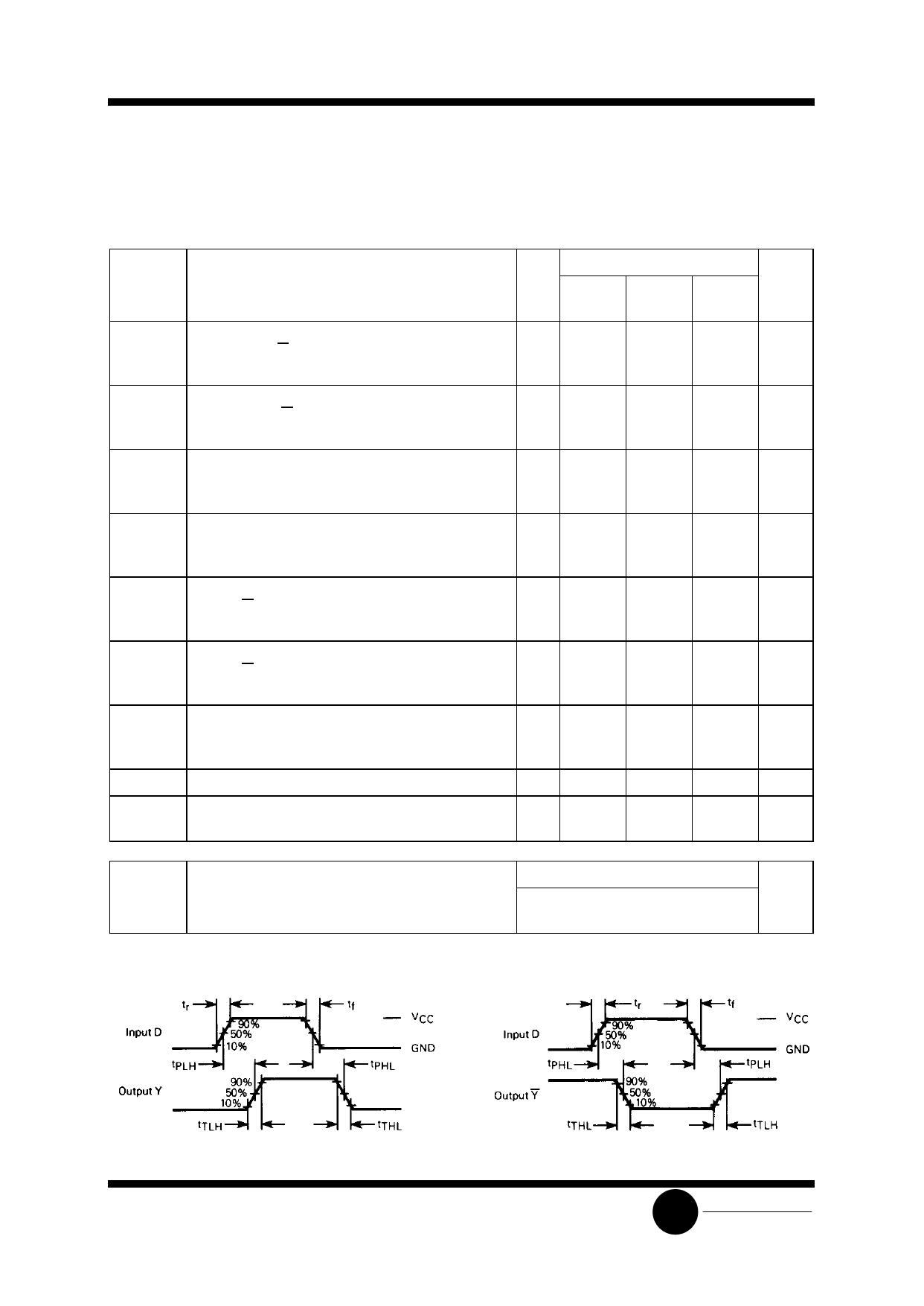
Figure 1. Switching Waveforms
Figure 2. Switching Waveforms
SLS
System Logic
Semiconductor
Share Link: