W78LE52-24 View Datasheet(PDF) - Winbond
Part Name
Description
View to exact match
W78LE52-24 Datasheet PDF : 22 Pages
| |||
Preliminary W78LE52
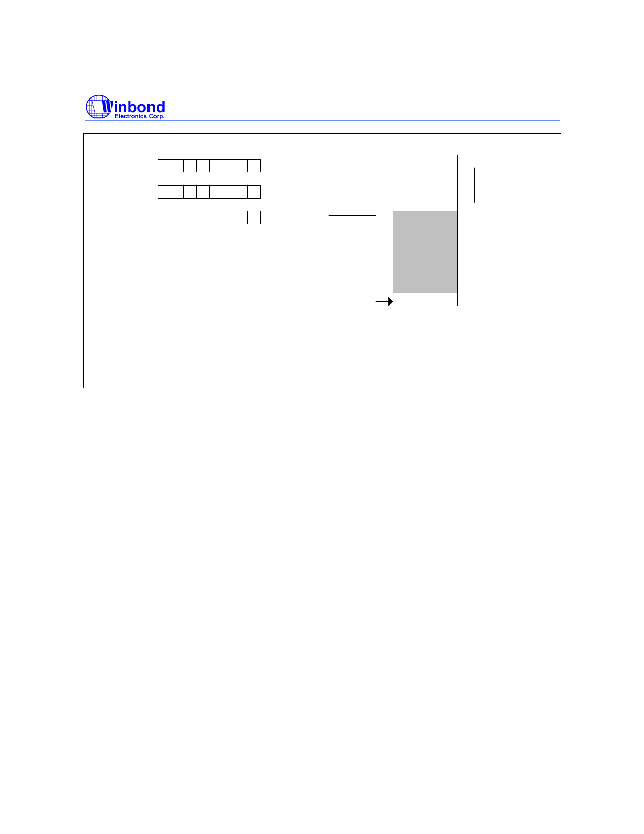
D7 D6 D5 D4 D3 D2 D1 D0
11011010
Company ID (#DAH)
8KB MTP ROM
0000h
11100000
Device ID (#E0H)
Program Memory
B7 Reserved B2 B1 B0
Security Bits
Reserved
B0 : Lock bit, logic 0 : active
B1 : MOVC inhibit,
logic 0 : the MOVC instruction in external memory
cannot access the code in internal memory.
logic 1 : no restriction.
B2 : Encryption
logic 0 : the encryption logic enable
logic 1 : the encryption logic disable
Security Register
B7 : Osillator Control
logic 0 : 1/2 gain
logic 1 : Full gain
Default 1 for all security bits.
Reserved bits must be kept in logic 1.
Special Setting Registers
1FFFh
0FFFFh
Lock bit
This bit is used to protect the customer's program code in the W78LE52. It may be set after the
programmer finishes the programming and verifies sequence. Once this bit is set to logic 0, both the
MTP ROM data and Special Setting Registers can not be accessed again.
MOVC Inhibit
This bit is used to restrict the accessible region of the MOVC instruction. It can prevent the MOVC
instruction in external program memory from reading the internal program code. When this bit is set
to logic 0, a MOVC instruction in external program memory space will be able to access code only in
the external memory, not in the internal memory. A MOVC instruction in internal program memory
space will always be able to access the ROM data in both internal and external memory. If this bit is
logic 1, there are no restrictions on the MOVC instruction.
Encryption
This bit is used to enable/disable the encryption logic for code protection. Once encryption feature is
enabled, the data presented on port 0 will be encoded via encryption logic. Only whole chip erase will
reset this bit.
- 11 -
Publication Release Date: January 1999
Revision A1
Share Link: 