PAS106BBB View Datasheet(PDF) - Unspecified
Part Name
Description
View to exact match
PAS106BBB Datasheet PDF : 15 Pages
| |||
PixArt Imaging Inc.
PAS106BCB -283/PAS106BBB-283
CMOS Image Sensor IC
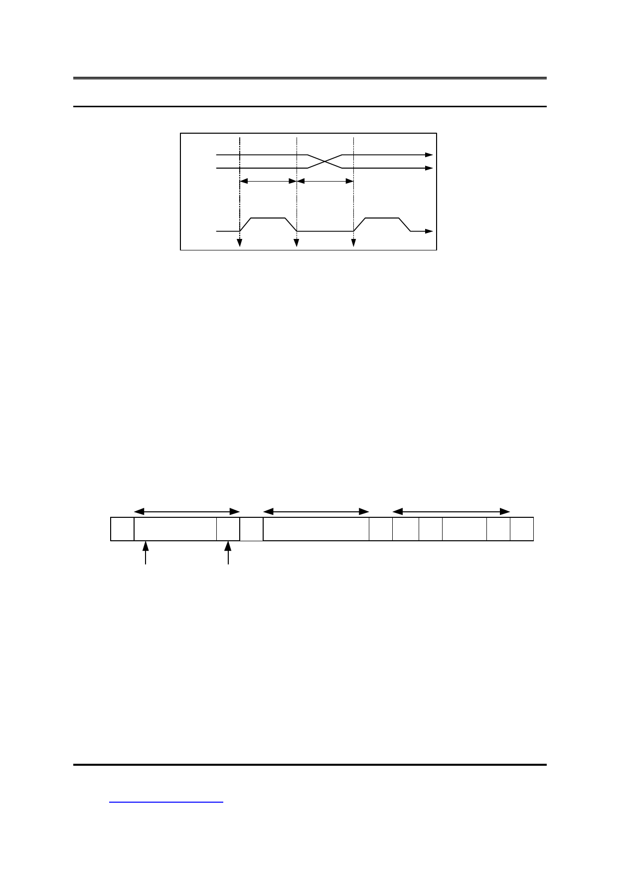
SDA
SCL
DATA
STABLE
DATA
CHANGE
ALLOWED
Fig 5.2 Valid Data
5.2 Data Transfer Format
5.2.1 Master transmits data to slave (write cycle)
§ S : Start
§ A : Acknowledge by slave
§ P : Stop
§ RW : The LSB of 1ST byte to decide whether current cycle is read or write cycle.
RW=1 read cycle, RW=0 write cycle.
§ SUBADDRESS : The address values of PAS106BCB-283/PAS106BBB-283 internal control
registers
(Please refer to PAS106BCB-283/PAS106BBB-283
register description)
1ST BYTE
S
SLAVE ID (7 BIT)
RW A
2ND BYTE
SUBADDRESS (8 BIT)
n BYTEs + A
A DATA A DATA
A
P
MSB
LSB=0
During write cycle, the master generates start condition and then places the 1st byte data that are combined
slave address (7 bits) with a read/write control bit to SDA line. After
slave(PAS106BCB-283/PAS106BBB-283) issues acknowledgment, the master places 2nd byte (sub-address)
data on SDA line. Again follow the PAS106BCB-283/PAS106BBB-283 acknowledgment, the master places
the 8 bits data on SDA line and transmit to PAS106BCB-283/PAS106BBB-283 control register (address was
assigned by 2nd byte). After PAS106BCB-283/PAS106BBB-283 issue acknowledgment, the master can
generate a stop condition to end of this write cycle. In the condition of multi-byte write, the
PAS106BCB-283/PAS106BBB-283 sub-address is automatically increment after each DATA byte transferred.
All rights strictly reserved any portion in this paper shall not be reproduced, copied or transformed to any other forms without permission.
7/14
PixArt Imaging Inc.
E-mail: fae_service@pixart.com.tw
V2.0, May 2002
Share Link: 