NLX2G66 View Datasheet(PDF) - ON Semiconductor
Part Name
Description
View to exact match
NLX2G66 Datasheet PDF : 12 Pages
| |||
VOS
0.1 mF
fin
NLX2G66
VIS
VOS
VCC
0.1 mF
VCC
fin
VCC
VCC
dB
GND
Meter
*Includes all probe and jig capacitance.
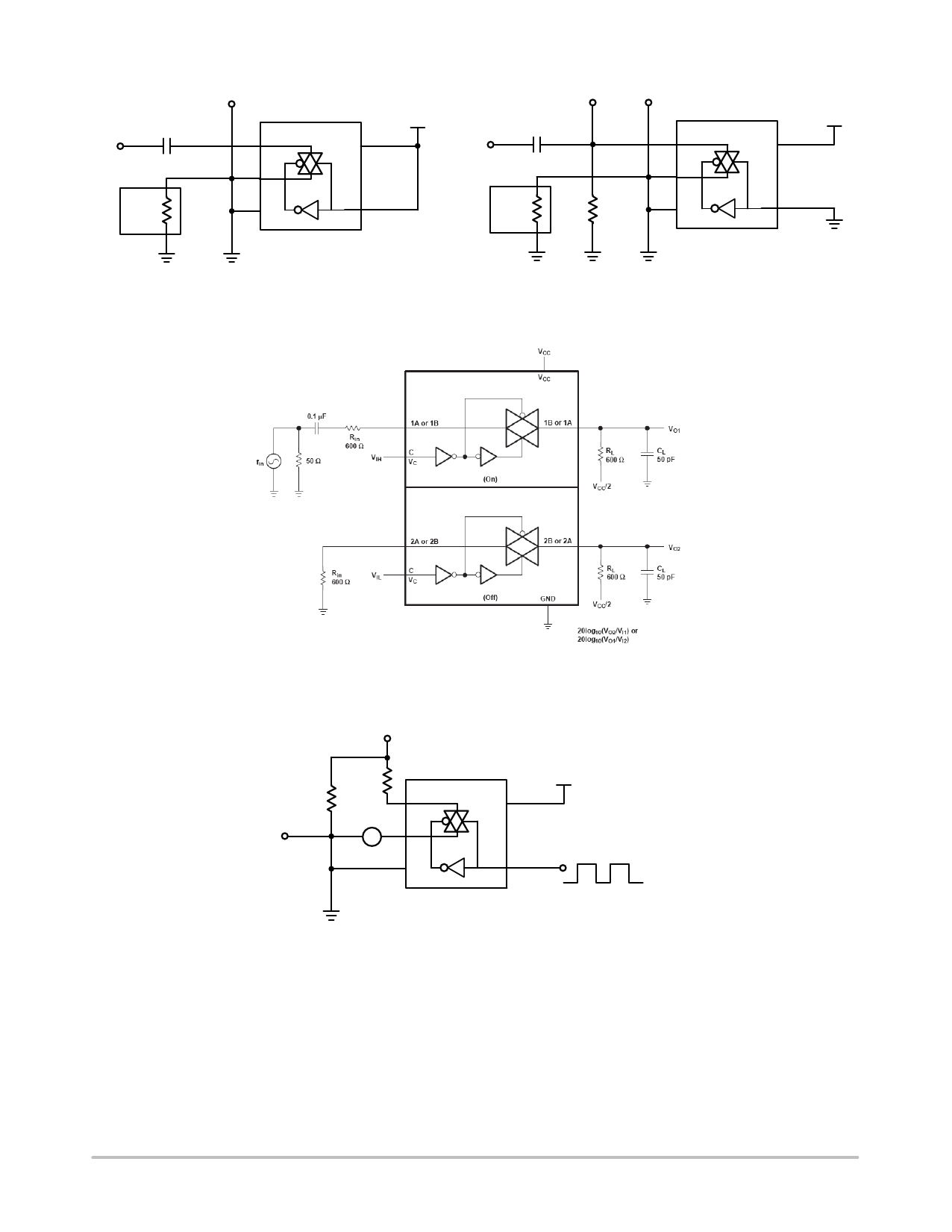
Figure 8. Maximum On−Channel Bandwidth
Test Set−Up
dB
Meter
RL
GND
*Includes all probe and jig capacitance.
Figure 9. Off−Channel Feedthrough Isolation
Test Set−Up
Figure 10. Crosstalk (between Switches)
(VCC)/2
RL
VOS
RL
IS
GND
VCC
VCC
VIN v 1 MHz
tr + tf + 2 ns
VCC
GND
*Includes all probe and jig capacitance.
Figure 11. Feedthrough Noise, ON/OFF Control
to Analog Out, Test Set−Up
http://onsemi.com
7
Share Link: 