NJU3505L View Datasheet(PDF) - Japan Radio Corporation
Part Name
Description
View to exact match
NJU3505L Datasheet PDF : 64 Pages
| |||
NJU3505
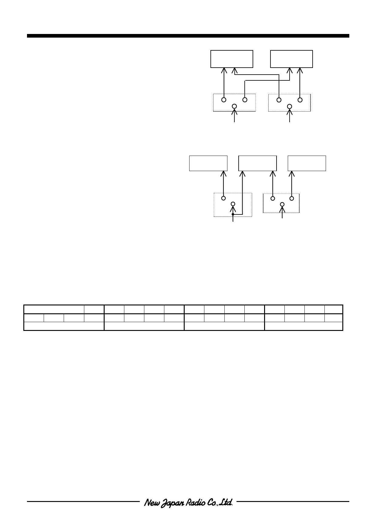
*5 Wiring of terminals
The mask option selects a terminal type
from VREF/PJ0, or ADCK/PJ1 as shown in
right.
ADC
PHY26
*6 Wiring of terminals
The mask option selects a terminal type
from EXTI/PK0, or CNTI/PK1 as shown
in right.
VREF / PJ0
ADCK / PJ1
Interrupt
Circuit
PHY27
Timer2
EXTI / PK0
CNTI / PK1
• ROM ADDRESSING REGISTER(PHY13, PHY14)
ROM ADDRESSING REGISTERS (PHY13. PHY14) indicates the address of ROM with Accumulator
and X'-reg for the data transference operation (TRM) from ROM to RAM.
The PHY13 and PHY14 condition are unknown on “RESET” operation. The lower a bit(b0) in PHY14 is
used as the ROM ADDRESSING and higher 3 bits(b1,b2,b3) are not used,
[ ROM ADDRESSING ]
no used
A12 A11 A10 A9 A8 A7 A6 A5 A4 A3 A2 A1 A0
b3 b2 b1 b0 b3 b2 b1 b0 b3 b2 b1 b0 b3 b2 b1 b0
PHY14
PHY13
X’
AC
- 14 -
Share Link: 