NCV8674DS50R4G(2008) View Datasheet(PDF) - ON Semiconductor
Part Name
Description
View to exact match
NCV8674DS50R4G Datasheet PDF : 11 Pages
| |||
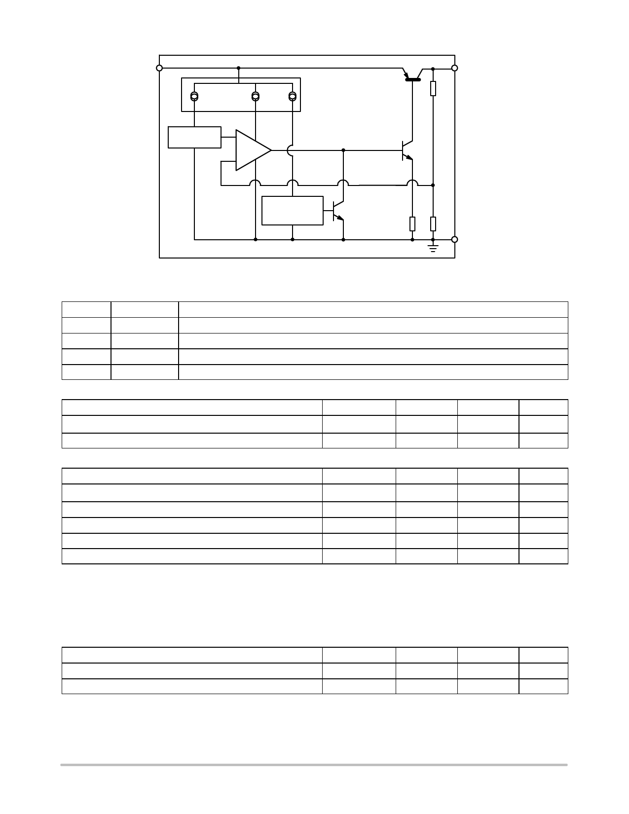
VIN
Bias Current
Generators
1.3 V
Reference
+
Error
Amp
-
NCV8674
VOUT
Thermal
Shutdown
GND
Figure 1. Block Diagram
PIN FUNCTION DESCRIPTION
Pin No.
Symbol
Function
1
VIN
Unregulated input voltage; (VOUT + 0.5 V) to 45 V.
2
GND
Ground; substrate.
3
VOUT
Regulated output voltage; collector of the internal PNP pass transistor.
TAB
GND
Ground; substrate and best thermal connection to the die.
OPERATING RANGE
Pin Symbol, Parameter
Symbol
Min
Max
Unit
VIN, DC Input Operating Voltage
Junction Temperature Operating Range
VIN
VOUT + 0.5 V
+45
V
TJ
−40
+150
_C
MAXIMUM RATINGS
Rating
Symbol
Min
Max
Unit
VIN, DC Voltage
VOUT, DC Voltage
Storage Temperature
ESD Capability, Human Body Model (Note 1)
ESD Capability, Machine Model (Note 1)
VIN
VOUT
Tstg
VESDHB
VESDMIM
−42
−0.3
−55
4000
200
+45
V
+16
V
+150
_C
−
V
−
V
Stresses exceeding Maximum Ratings may damage the device. Maximum Ratings are stress ratings only. Functional operation above the
Recommended Operating Conditions is not implied. Extended exposure to stresses above the Recommended Operating Conditions may affect
device reliability.
1. This device series incorporates ESD protection and is tested by the following methods:
ESD HBM tested per AEC−Q100−002 (EIA/JESD22−A 114C)
ESD MM tested per AEC−Q100−003 (EIA/JESD22−A 115C)
Thermal Resistance
Parameter
Junction−to−Ambient(Note 2)
Junction−to−Case
2. 1 oz., 1 in2 copper area.
Symbol
Min
Max
Unit
RqJA
RqJC
−
40
°C/W
−
4.0
°C/W
http://onsemi.com
2
Share Link: 