MC74HCT08ADG View Datasheet(PDF) - ON Semiconductor
Part Name
Description
View to exact match
MC74HCT08ADG Datasheet PDF : 7 Pages
| |||
MC74HCT08A
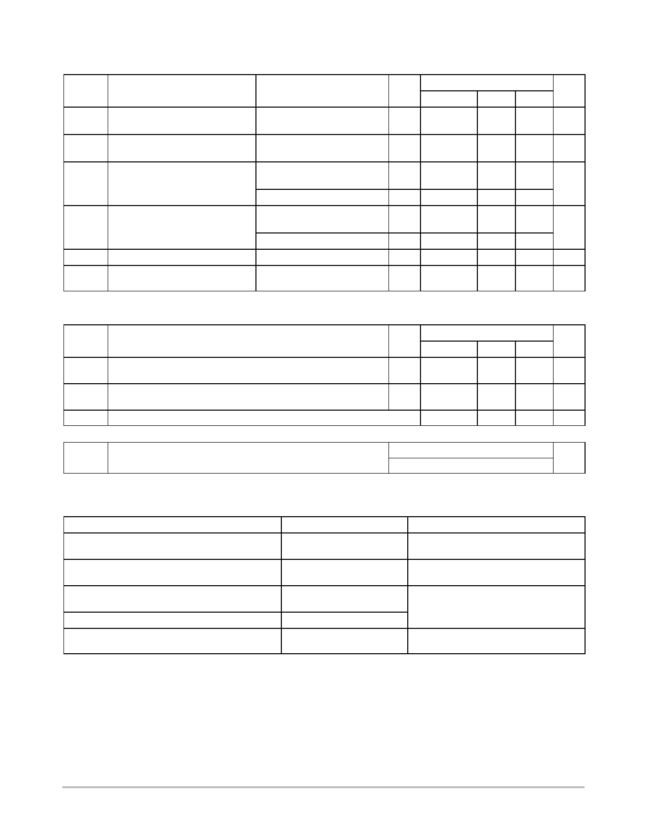
DC CHARACTERISTICS (Voltages Referenced to GND)
Symbol
Parameter
Condition
Guaranteed Limit
VCC
V −55 to 25°C ≤85°C ≤125°C Unit
VIH
Minimum High−Level Input Voltage Vout = 0.1 V or VCC −0.1 V
|Iout| ≤ 20 mA
4.5 to
2.0
5.5
2.0
2.0
V
VIL
Maximum Low−Level Input Voltage Vout = 0.1 V or VCC − 0.1 V
|Iout| ≤ 20 mA
4.5 to
0.8
5.5
0.8
0.8
V
VOH Minimum High−Level Output Voltage Vin = VIH or VIL
|Iout| ≤ 20 mA
4.5
4.4
5.5
5.4
4.4
4.4
V
5.4
5.4
Vin =VIH or VIL |Iout| ≤ 4.0 mA 4.5
VOL
Maximum Low−Level Output Voltage Vin = VIH or VIL
4.5
|Iout| ≤ 20mA
5.5
3.98
0.1
0.1
3.84 3.70
0.1
0.1
V
0.1
0.1
Iin
Maximum Input Leakage Current
ICC
Maximum Quiescent Supply
Current (per Package)
Vin = VIH or VIL |Iout| ≤ 4.0 mA 4.5
Vin = VCC or GND
5.5
Vin = VCC or GND
5.5
Iout = 0 mA
0.26
±0.1
1.0
0.33 0.40
±1.0
±1.0
mA
10
40
mA
AC CHARACTERISTICS (CL = 50 pF, Input tr = tf = 6 ns, VCC = 5.0 V ± 10%)
Symbol
Parameter
tPLH, Maximum Propagation Delay, Input A or B to Output Y
tPLH
tPHL (Figures 3 and 4)
tPHL
tTLH,
tTHL
Maximum Output Transition Time, Any Output
(Figures 3 and 4)
Cin
Maximum Input Capacitance
Guaranteed Limit
VCC
V −55 to 25°C ≤85°C ≤125°C Unit
5.0
15
17
19
22
ns
21
26
5.0
15
19
22
ns
10
10
10
pF
Typical @ 25°C, VCC = 5.0 V, VEE = 0 V
CPD Power Dissipation Capacitance (Per Buffer)*
20
pF
*Used to determine the no−load dynamic power consumption: PD = CPD VCC2f + ICC VCC.
ORDERING INFORMATION
Device
Package
Shipping†
MC74HCT08ANG
PDIP−14
(Pb−Free)
25 Units / Rail
MC74HCT08ADG
SOIC−14
(Pb−Free)
55 Units / Rail
MC74HCT08ADR2G
MC74HCT08ADTR2G
SOIC−14
(Pb−Free)
TSSOP−14*
2500/Tape & Reel
MC74HCT08AFELG
SOEIAJ−14
(Pb−Free)
2000/Tape & Reel
†For information on tape and reel specifications, including part orientation and tape sizes, please refer to our Tape and Reel Packaging
Specifications Brochure, BRD8011/D.
*This package is inherently Pb−Free.
http://onsemi.com
3
Share Link: 