74HC365 View Datasheet(PDF) - STMicroelectronics
Part Name
Description
View to exact match
74HC365 Datasheet PDF : 14 Pages
| |||
M74HC365
Hex bus buffer with 3-state outputs (non-inverting)
Datasheet - production data
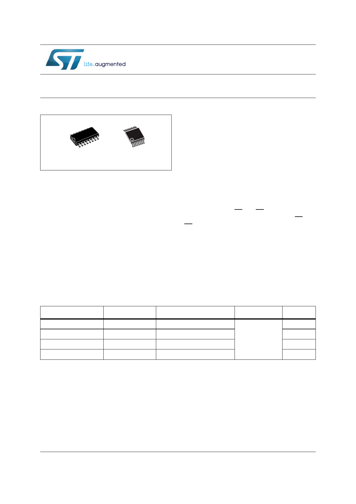
SO16
TSSOP16
• Pin and function compatible with 74 series 365
• ESD performance
– HBM: 2 kV
– MM: 200 V
– CDM: 1 kV
Description
Features
• High-speed:
tPD = 10 ns (typ.) at VCC = 6 V
• Low power dissipation:
ICC = 4 μA (max.) at TA = 25 °C
• High noise immunity:
VNIH = VNIL = 28 % VCC (min)
• Symmetrical output impedance:
|IOH| = IOL = 6 mA (min.)
• Balanced propagation delays:
tPLH ≅ tPHL
• Wide operating voltage range:
VCC (opr) = 2 V to 6 V
The M74HC365 is an advanced high-speed
CMOS hex bus buffer (3-state) fabricated with
silicon gate C2MOS technology.
All six buffers are controlled by the combination of
two enable inputs (G1 and G2). All outputs of
these buffers are enabled only when both G1 and
G2 inputs are held low. Under all other conditions
these outputs are disabled in a high-impedance
state.
The M74HC365 has non-inverting outputs.
All inputs are equipped with protection circuits
against static discharge and transient excess
voltage.
Order code
Table 1. Device summary
Temp. range
Package
Packing
Marking
M74HC365RM13TR
M74HC365YRM13TR(1)
M74HC365TTR
M74HC365YTTR(1)
-55 °C to 125 °C
-40 °C to 125 °C
-55 °C to 125 °C
-40 °C to 125 °C
S016
SO16 (automotive grade)
TSSOP16
TSSOP16 (automotive grade)
Tape and reel
74HC365
74HC365Y
HC365
HC365Y
1. Qualification and characterization according to AEC Q100 and Q003 or equivalent, advanced screening according to AEC
Q001 and Q002 or equivalent.
January 2014
This is information on a product in full production.
DocID1948 Rev 3
1/14
www.st.com
Share Link: 