AT27LV520(1998) View Datasheet(PDF) - Atmel Corporation
Part Name
Description
View to exact match
AT27LV520
(Rev.:1998)
(Rev.:1998)
Atmel Corporation

AT27LV520 Datasheet PDF : 10 Pages
| |||
AT27LV520
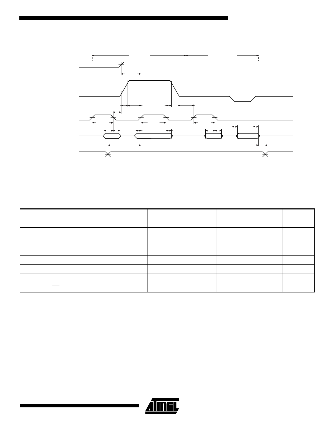
AC Programming Characteristics*
TA = 25 ± 5°C, VCC = 6.5 ± 0.25V, OE/VPP = 13.0 ± 0.25V
Symbol Parameter(1)
Test Conditions
Limits
Min
Max
Units
tALE
tLAS
tLAH
tLP
tOES
tOEH
tDS
tDH
tPW
tVR
tVCS
tOE
tDFP
tAS
tAH
tPRT
Address Latch Enable Width
500
Latched Address Setup Time
100
Latched Address Hold Time
100
ALE Low to OE/VPP High Voltage Delay
2
OE/VPP Setup Time
OE/VPP Hold Time
Input Rise and Fall Times
2
(10% to 90%) 20 ns
2
Data Setup Time
Data Hold Time
Input Pulse Levels
2
0.45V to 2.4V
2
ALE Program Pulse Width(2)
OE/VPP Recovery Time
47.5
Input Timing Reference Level
0.8V to 2.0V
2
VCC Setup Time
2
Data Valid from OE/VPP
Output Timing Reference Level
0.8V to 2.0V
OE/VPP High to Output Float Delay(4)
0
Address Setup Time
2
Address Hold Time
0
OE/VPP Pulse Rise Time During
Programming
50
ns
ns
ns
µs
µs
µs
µs
µs
52.5
µs
µs
µs
150
ns
130
ns
µs
µs
ns
Notes:
1. VCC must be applied simultaneously or before OE/VPP and removed simultaneously or after OE/VPP.
2. Program Pulse width tolerance is 50 µsec ± 5%.
3. This parameter is only sampled and is not 100% tested. Output Float is defined as the point where data is no longer driven
— see timing diagram.
Atmel’s 27LV520 Integrated Product Identification Code
Codes
Manufacturer
Device Type
Pins
Hex
A8
AD7
AD6
AD5
AD4
AD3
AD2
AD1
AD0
Data
0
0
0
0
1
1
1
1
0
1E
1
1
0
0
1
1
1
0
1
9D
7
Share Link: