LR38630 View Datasheet(PDF) - Sharp Electronics
Part Name
Description
View to exact match
LR38630 Datasheet PDF : 20 Pages
| |||
LR38630
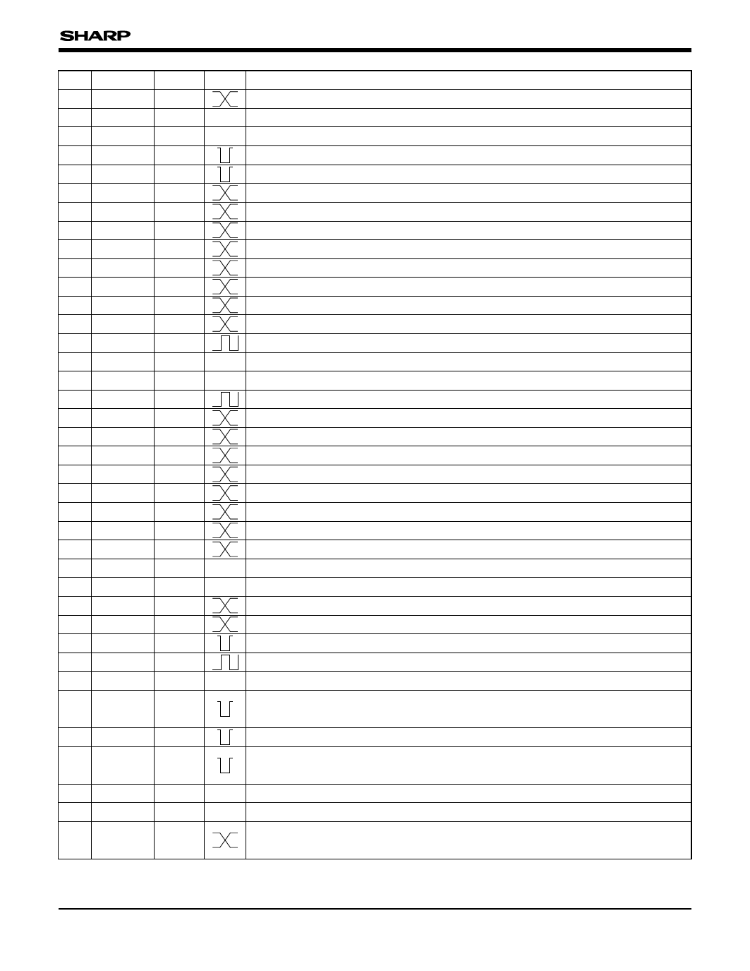
PIN NO. SYMBOL I/O POLARITY
DESCRIPTION
40 ADD0
IO4M
Address output to drive an external SRAM.
41 TST1
IC
A test pin. Connected to GND.
42 TST2
IC
A test pin. Connected to GND.
43 OE
OBF4M
Output enable to drive an external SRAM.
44 WE
OBF4M
Write enable to drive an external SRAM.
45 MDIO7 IO4MU
Address output to drive an external SRAM.
46 MDIO6 IO4MU
Address output to drive an external SRAM.
47 MDIO5 IO4MU
Address output to drive an external SRAM.
48 MDIO4 IO4MU
Address output to drive an external SRAM.
49 MDIO3 IO4MU
Address output to drive an external SRAM.
50 MDIO2 IO4MU
Address output to drive an external SRAM.
51 MDIO1 IO4MU
Address output to drive an external SRAM.
52 MDIO0 IO4MU
Address output to drive an external SRAM.
53 EXMCK
IC
External clock input.
54 GND
–
A grounding pin.
55 VDD
–
Supply of +3.0 V power.
56 RCLK OBF4M
Clock output for digital video output signal.
57 DATA7 OBF4M
Data input/output to drive an external SRAM.
58 DATA6 OBF4M
Data input/output to drive an external SRAM.
59 DATA5 OBF4M
Data input/output to drive an external SRAM.
60 DATA4 OBF4M
Data input/output to drive an external SRAM.
61 DATA3 OBF4M
Data input/output to drive an external SRAM.
62 DATA2 OBF4M
Data input/output to drive an external SRAM.
63 DATA1 OBF4M
Data input/output to drive an external SRAM.
64 DATA0 OBF4M
Data input/output to drive an external SRAM.
65 GND
–
A grounding pin.
66 VDD
–
Supply of +3.0 V power.
67 CTLDIN IC
Serial data input.
68 CTLDOUT OBF4M
Serial data input.
69 CTLDEN IC
The rising edge enables the serial data to be available.
70 CTLDCK IC
Clock input to set the data.
71 STANDBY IC
High level puts this IC and LZ34C10 in standby mode.
72 HREF OBF4M
Horizontal blanking pulse output keeping high level during the effective image
period.
73 OLSTEN OBF4M
Horizontal pulse output going to low level when starting in horizontal.
74 VS
OBF4M
Vertical blanking pulse output keeping high level during the effective image
period.
75 GND
–
A grounding pin.
76 VDD
–
Supply of +3.0 V power.
77 EEPDA IO4M
Data input/output to/from EEPROM.
Going to high-impedance with high level of pin 80.
5
Share Link: 