LR38617 View Datasheet(PDF) - Sharp Electronics
Part Name
Description
View to exact match
LR38617 Datasheet PDF : 9 Pages
| |||
LR38617
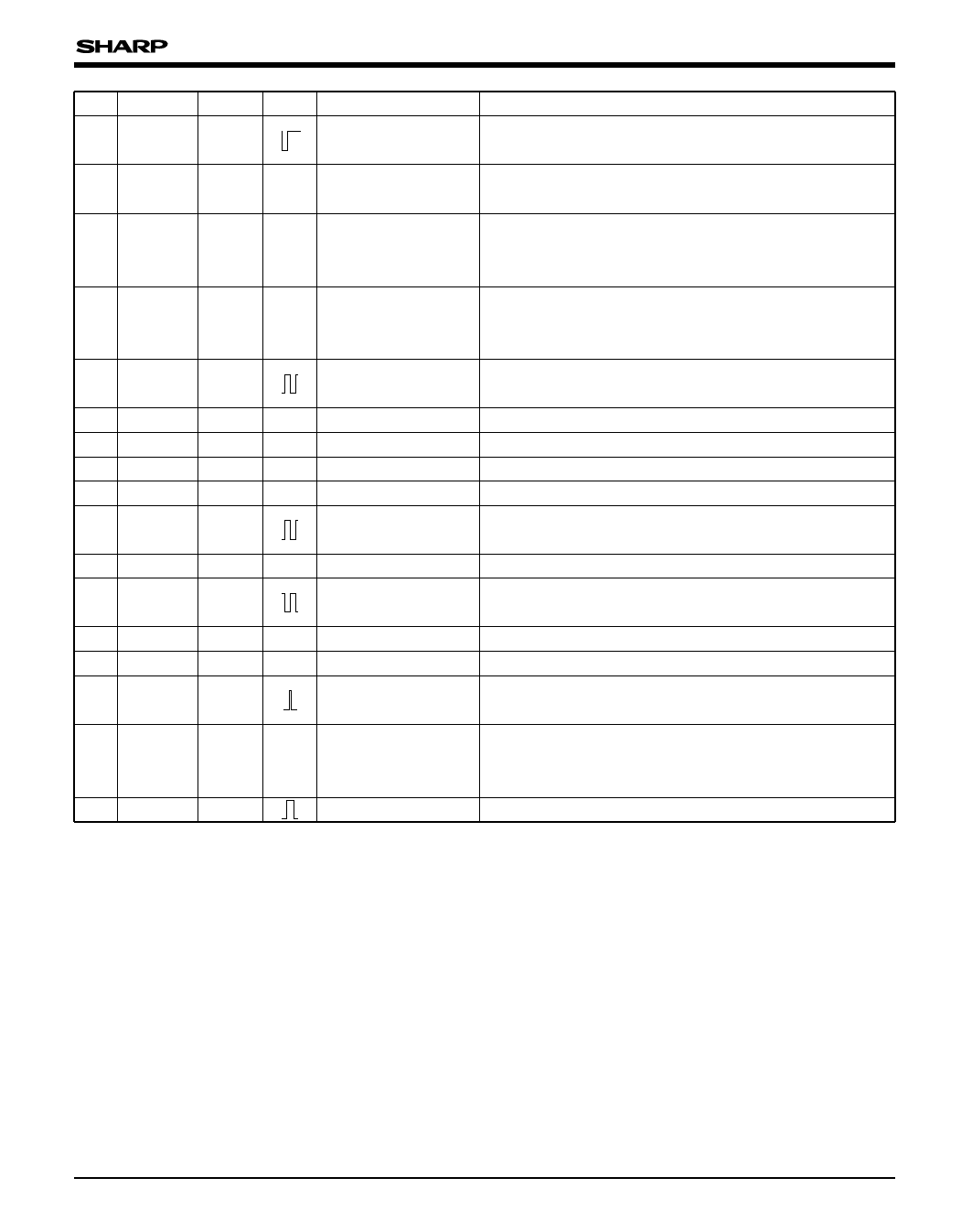
PIN NO. SYMBOL IO SYMBOL POLARITY
PIN NAME
32 HD
IC3
Horizontal drive
pulse input
33 ED0
ICSU3 – Strobe pulse input
34 ED1
Shift register clock
ICSU3 –
input
35 ED2
36 ID
37 TST1
38 NC
39 NC
40 VDD4
41 FH1
42 GND
43 FH2
44 VDD4
45 NC
46 FR
Shift register data
ICSU3 –
input
O3
ICD4 –
–
–
–
–
–
–
O6MA43
–
–
O6MA43
–
–
–
–
Line index pulse
output
Test pin 1
No connection
No connection
Power supply
Horizontal transfer
pulse output 1
Ground
Horizontal transfer
pulse output 2
Power supply
No connection
O6MA43
Reset pulse output
47 CCD
ICU4 – CCD selection input
48 SHTR
O3
Trigger output
IC3
ICU3
ICSU3
ICU4
ICD4
: Input pin (CMOS level)
: Input pin (CMOS level with pull-up resistor)
: Input pin (CMOS schmitt-trigger level with pull-up
resistor)
: Input pin (CMOS level with pull-up resistor)
: Input pin (CMOS level with pull-down resistor)
DESCRIPTION
An input pin for reference of horizontal pulse.
Connect to HD pin of DSP IC.
An input pin for the strobe pulse, to control the functions
of LR38617. For details, see "Serial Data Control".
An input pin for the clock of the shift register, to control
the functions of LR38617. For details, see "Serial Data
Control".
An input pin for the data of the shift register, to control
the functions of LR38617. For details, see "Serial Data
Control".
The pulse is used in the color separator.
The signal switches between high and low at every line.
A test pin. Set open or to L level in normal mode.
No connection.
No connection.
Supply of +4.5 V power.
A horizontal transfer pulse for the CCD.
Connect to ØH1 pin of the CCD.
A grounding pin.
A horizontal transfer pulse for the CCD.
Connect to ØH2 pin of the CCD.
Supply of +4.5 V power.
No connection.
A pulse to reset the charge of output circuit.
The output phase of FR is selected by serial data.
An input pin to select CCD.
L level
: Aspect ratio 4 : 3 CCD
H level or open : Aspect ratio 3 : 2 CCD
A trigger pulse for effective signal period.
O3
: Output pin (output high level is VDD3.)
O6MA3 : Output pin (output high level is VDD3.)
O6MA43 : Output pin (output high level is VDD4.)
OSCI3 : Input pin for oscillation
OSCO3 : Output pin for oscillation
5
Share Link: 