VSC6424 View Datasheet(PDF) - Vitesse Semiconductor
Part Name
Description
View to exact match
VSC6424 Datasheet PDF : 18 Pages
| |||
500 Mb/s Video
Shift Register IC
VITESSE
SEMICONDUCTOR CORPORATION
Preliminary Datasheet
VSC6424
HBLANK or VBLANK must be driven low for at least one clock cycle two clock cycles before the desired
point of blanking. See Figure 6 for a timing illustration of this function.
Retimer
The chip also contains a retimer function. This function works in DEMUX mode. The RETIME signal is
routed to DOUT<7> through a flip-flop. The flip-flop is internally clocked by the low speed ECL output clock
(CLKE). This function is depicted in the detailed block diagram (Figure 3) below. See Figure 5 for a timing
illustration.
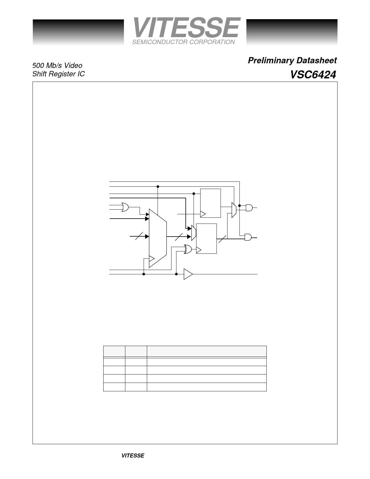
OEN
MODE
AEN/RETIME
A<0:4>
HBLANK
VBLANK
S<0:2>
OPS
CLK
Figure 2: Multiplexer Detailed Block Diagram
CLKE
40 MUX 8
Retimer
7
Output 8
Latch
DOUT<7>
DOUT<0:6>
High
Speed
Interface
(ECL)
CLKOUT
Termination
It is recommended to leave all unused ECL outputs floating. It is recommended that unused ECL inputs be
terminated low (-2V supply). Refer to the following table recommended input termination for all levels.
Table 4: Input Termination Recommendations
Type
ECL
ECL
TTL
TTL
State
High
Low
High
Low
Input
ground via a diode
-2V supply
+3.3V supply
Ground
Page 6
© VITESSE SEMICONDUCTOR CORPORATION
741 Calle Plano, Camarillo, CA 93012 • 805/388-3700 • FAX: 805/987-5896
G52236-0, Rev 3.0
7/13/99
Share Link: 