LB1862 View Datasheet(PDF) - SANYO -> Panasonic
Part Name
Description
View to exact match
LB1862 Datasheet PDF : 6 Pages
| |||
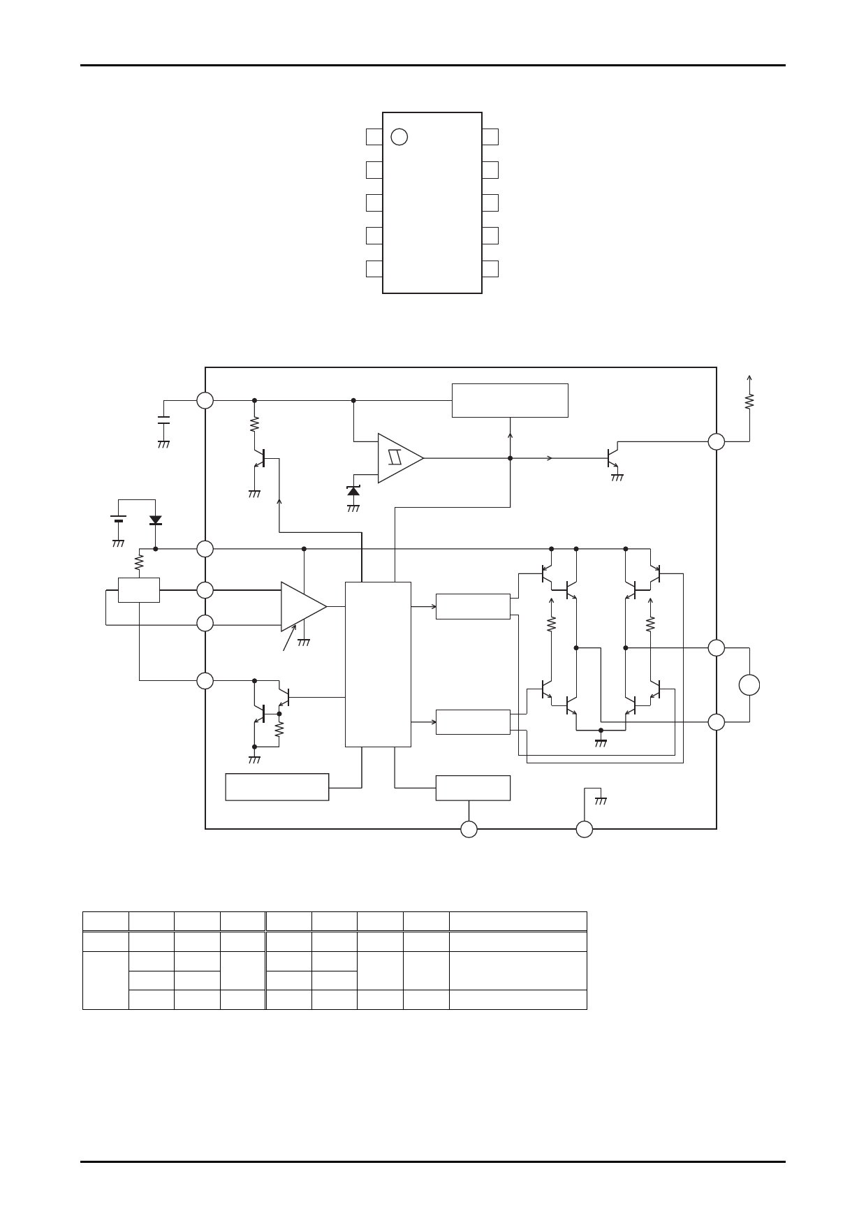
Pin Assignment
Block Diagram
CT
0.47 to 1µF
LB1862
IN− 1
IN+ 2
10 RD
9 HB
CT 3
OUT1 4
GND 5
LB1862
8 ST
7 VCC
6 OUT2
Top view
Charge / Discharge
circuit
VCC
Discharge
pulse
IN+
HALL
IN−
Hysteresis amplifier
HB
Control
circuit
Delay circuit
Delay circuit
Thermal protection
circuit
START/STOP
ST
GND
Truth Table
ST
IN-
IN+
H
-
-
H
L
L
L
H
-
-
CT
OUT1 OUT2
RD
HB
Mode
-
OFF OFF OFF OFF
Standby
H
L
L
L
L
L
H
Rotating
H
OFF OFF OFF
L
Lockup protection activated
Latch-type RD output is Low during rotation and High during stop.
RD
OUT2
M
OUT1
No.6208-3/6
Share Link: 