LB11988V(2006) View Datasheet(PDF) - SANYO -> Panasonic
Part Name
Description
View to exact match
LB11988V Datasheet PDF : 7 Pages
| |||
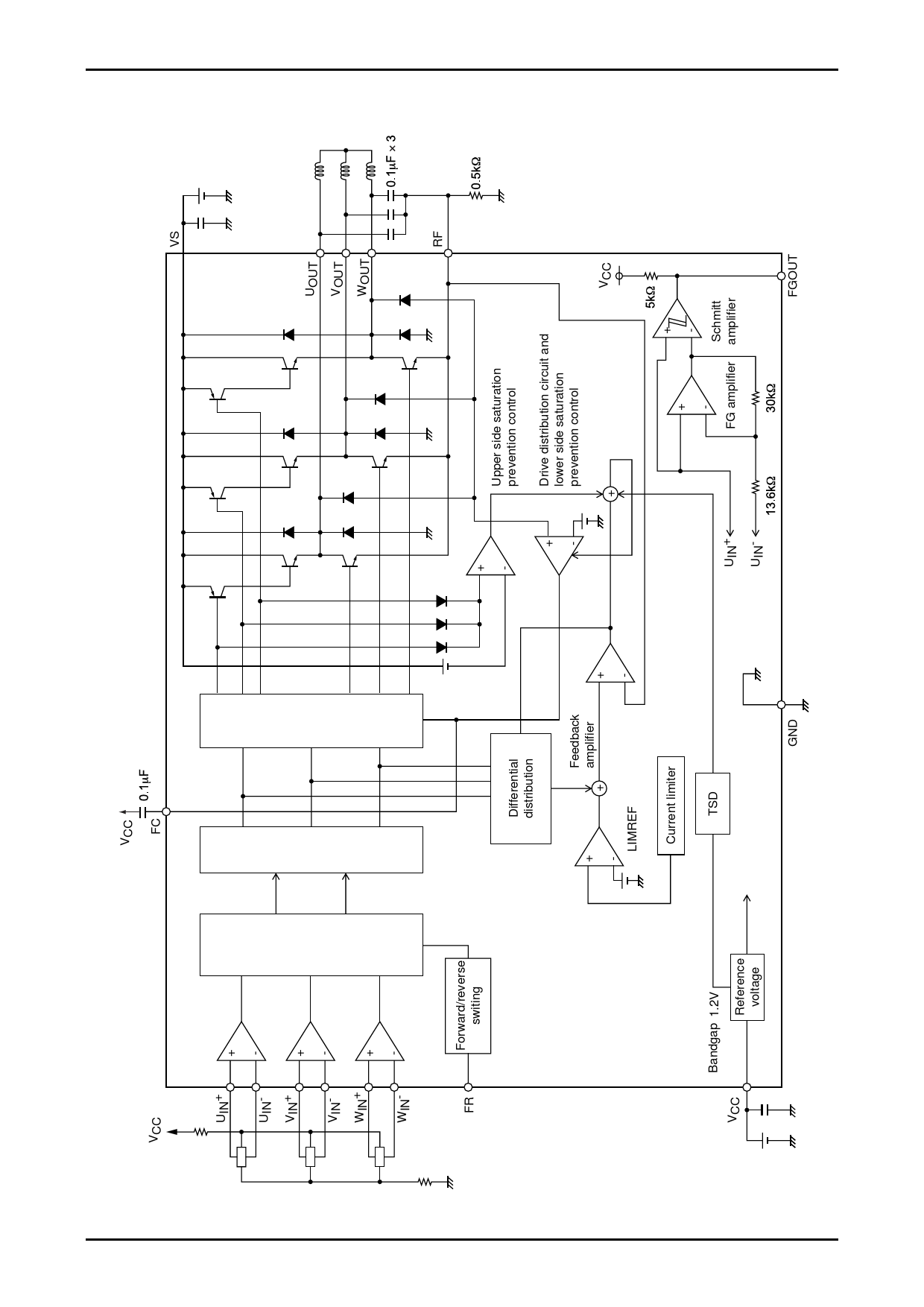
LB11988V
Pin Functions
Pin
Pin Name
No.
GND
6
UIN+, UIN- 10,11
Pin Functions
GND for others than the output transistor.
Minimum potential of output transistor is
at RF pin.
U-phase Hall device input pin;
logic “H” presents IN+>IN-
VIN+, VIN-
12,14
V-phase Hall device input pin;
logic “H” presents IN+>IN-
Input/Output Equivalent Circuit
Each (+) input
10
12
15 200Ω
Each (-) input
11
14
200Ω 16
WIN+,WIN-
15,16
W-phase Hall device input pin;
logic “H” presents IN+>IN-
UOUT
VOUT
WOUT
RF
VS
FR
23
U-phase output pin.
24
V-phase output pin.
1
W-phase output pin.
(Built-in spark killer diode)
20
Output current detection pin.
Connecting Rf between this pin and GND
activates current limiting circuit. Then the
lower over-saturation prevention circuit is
activated in accordance with this pin
voltage. Since the over-saturation
prevention level is set with this voltage,
the lower over-saturation prevention effect
may deteriorate in the high current range
if the Rf value is reduced to an extremely
low level.
19
Power supply pin for supplying power to
output section in IC.
5
Forward/Reverse switching pin.
19 VS
Each OUT
23 24 1
200Ω
VCC
Lower oversaturation
prevention circuit
block
20 RF
VCC
FR 5
200Ω
FC
9
Frequency characteristics compensation
pin for over-saturation prevention circuit
loop.
VCC
9 FC
Continued on next page.
No.A0377-4/7
Share Link: 