GP30B120KD-E View Datasheet(PDF) - International Rectifier
Part Name
Description
View to exact match
GP30B120KD-E Datasheet PDF : 12 Pages
| |||
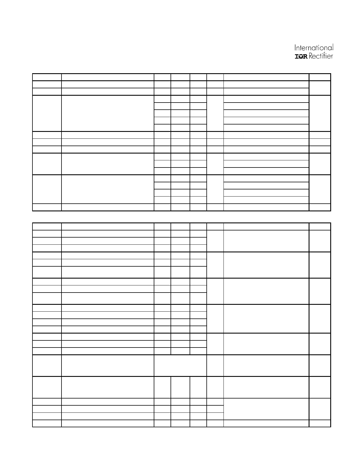
IRGP30B120KD-E
Electrical Characteristics @ TJ = 25°C (unless otherwise specified)
P a ra m e te r
V (BR)CES
Collector-to-Em itter Breakdown Voltage
∆V (BR )CE S / ∆T j T em p e ra tu re C o e ff. o f B re a kd o wn V o lta g e
M in .
1200
V CE(on)
Collector-to-Em itter Saturation
V o lta g e
V GE(th)
∆V G E (th) / ∆T j
g fe
G ate Threshold Voltage
Tem perature Coeff. of Threshold Voltage
Forward Transconductance
4 .0
1 4 .8
IC E S
Zero G ate Voltage Collector Current
V FM
Diode Forward Voltage Drop
IG E S
G ate-to-Em itter Leakage Current
Typ.
+1.2
2 .2 8
2 .4 6
3 .4 3
2 .7 4
2 .9 8
5 .0
- 1.2
1 6 .9
325
1 .7 6
1 .8 6
1 .8 7
2 .0 1
Max. Units
C o n d itio n s
2 .4 8
V
V /°C
V GE = 0 V ,Ic =2 50 µ A
V GE = 0 V , Ic = 1 m A ( 2 5 -1 2 5 oC )
IC = 25A , V GE = 15V
2 .6 6
IC = 30A , V GE = 15V
4.00 V IC = 60A , V GE = 15V
3 .1 0
IC = 25A , V GE = 15V , TJ = 125°C
3 .3 5
IC = 30A , V GE = 15V , TJ = 125°C
6 .0
1 9 .0
V
m V/oC
S
V CE = V GE, IC = 25 0 µ A
V CE = V GE, IC = 1 m A ( 2 5 -1 2 5 oC )
V CE = 50 V , IC = 25 A , P W =80 µ s
250
VGE = 0V,VCE = 1200V
675 µA VGE = 0v, VCE = 1200V, TJ =125°C
2000
VGE = 0v, VCE = 1200V, TJ =150°C
2 .0 6
IC = 25A
2.17 V IC = 30A
2 .1 8
IC = 25A , TJ = 125°C
2 .4 0
IC = 30A , TJ = 125°C
±100 nA VGE = ±20V
F ig .
5, 6
7, 9
10
11
9,10,11,12
8
Switching Characteristics @ TJ = 25°C (unless otherwise specified)
P a ra m e te r
Min. Typ. Max. Units
C o n d itio n s
F ig .
Qg
Q ge
Q gc
E on
E off
E tot
E on
E off
E tot
td (o n )
tr
td(off)
tf
Total Gate charge (turn-on)
G ate - Em itter Charge (turn-on)
G ate - Collector Charge (turn-on)
Turn-O n Switching Loss
Turn-O ff Switching Loss
Total Switching Loss
Turn-on Switching Loss
Turn-off Switching Loss
Total Switching Loss
Turn - on delay tim e
Rise tim e
Turn - off delay tim e
Fall tim e
169
19
82
1066
1493
254
29
123
1250
1800
2559 3050
1660 1856
2118 2580
3778 4436
50 65
25 35
210 230
60 75
IC = 25A
nC VCC =600V
VGE = 15V
IC = 25A , V CC = 600V
µ J V GE = 1 5 V , R g = 5 Ω, L =200µH
TJ = 25oC, Energy losses include tail
and diode reverse recovery
Ic =2 5A , V CC=6 00 V
µ J V GE = 1 5 V , R g = 5 Ω, L =200µH
TJ = 125oC, Energy losses include tail
and diode reverse recovery
Ic =2 5A , V CC=6 00 V
n s V GE = 1 5 V , R g = 5 Ω, L =200µH
T J = 12 5 oC ,
23
CT 1
CT 4
WF1
WF2
13, 15
CT 4
WF1 & 2
14, 16
CT 4
WF1
WF2
C ies
C oes
C res
RBSOA
Input Capacitance
O utput Capacitance
Reverse Transfer Capacitance
Reverse bias safe operating area
SCSOA
Short Circuit Safe O perating Area
E rec
Reverse recovery energy of the diode
trr
Diode Reverse recovery tim e
Irr
Peak Reverse Recovery Current
Le
Internal Em itter Inductance
2200
210
85
FULL SQUARE
10 ---- ----
1820
300
34
13
2400
38
VGE = 0V
pF VCC = 30V
f = 1.0 MHz
TJ =1 50 oC , Ic = 1 2 0A
VCC = 1000V, VP = 1200V
R g = 5 Ω, V GE = + 1 5 V to 0 V
T J = 15 0 oC
µs VCC = 900V,VP = 1200V
R g = 5 Ω, V GE = + 1 5 V to 0 V
µ J T J = 12 5 oC
n s V CC = 60 0 V , Ic = 25 A
A V GE = 1 5 V , R g = 5 Ω, L =200µH
nH M easured 5 m m from the package.
22
4
CT 2
CT 3
WF4
17,18,19
20, 21
CT 4, WF3
2
www.irf.com
Share Link: 