IPS511 View Datasheet(PDF) - International Rectifier
Part Name
Description
View to exact match
IPS511 Datasheet PDF : 12 Pages
| |||
IPS511/IPS511S
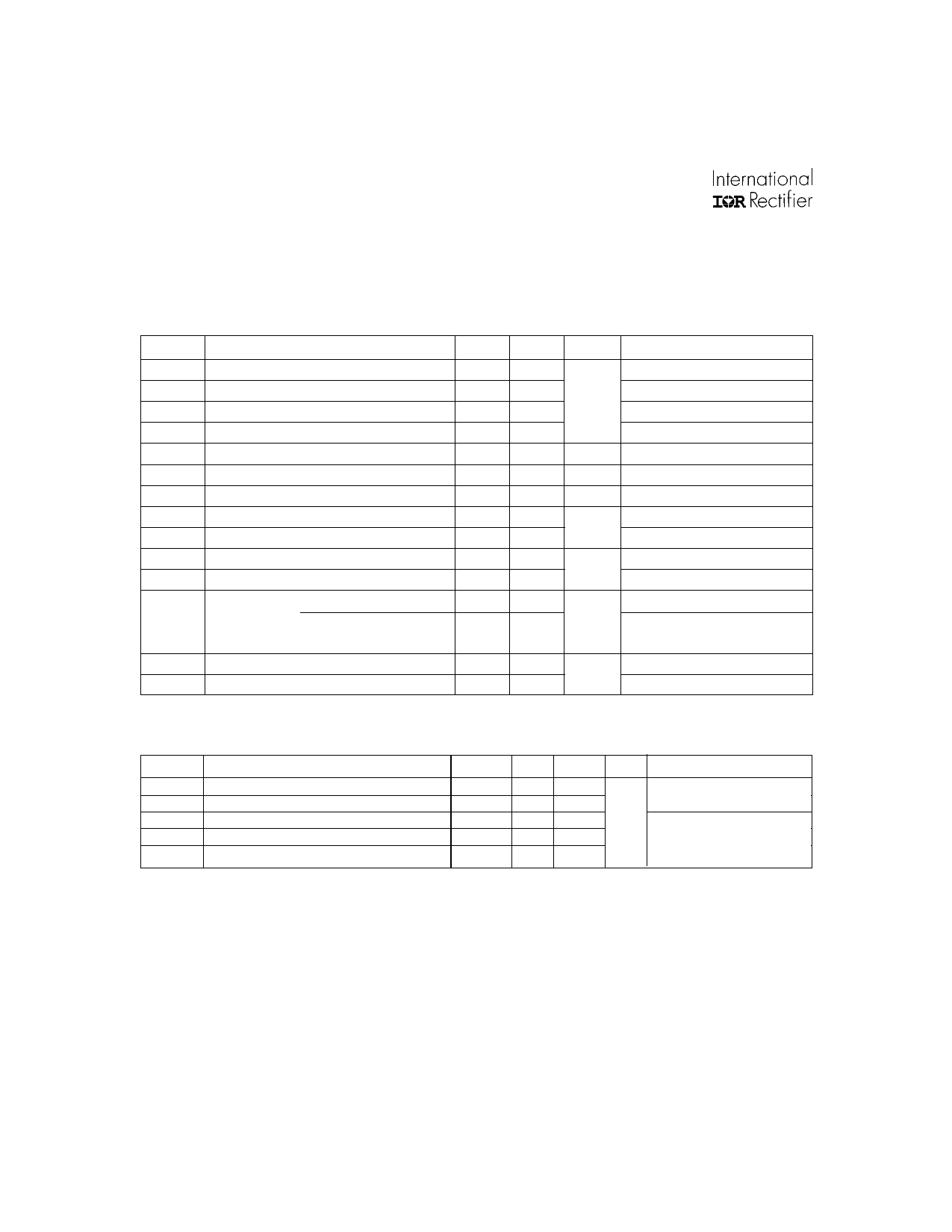
Absolute Maximum Ratings
Absolute maximum ratings indicate sustained limits beyond which damage to the device may occur. All voltage parameters
are referenced to GROUND lead. (Tj = 25oC unless otherwise specified).
Symbol Parameter
Min.
Vout
Voffset
Vin
Vcc max
Iin, max.
Maximum output voltage
Vcc-50
Maximum logic ground to load ground offset Vcc-50
Maximum Input voltage
-0.3
Maximum Vcc voltage
—
Maximum IN current
-5
Vdg
Maximum diagnostic output voltage
-0.3
Idg, max Maximum diagnostic output current
-1
Isd cont. Diode max. permanent current (1)
—
Isd pulsed Diode max. pulsed current (1)
—
ESD1 Electrostatic discharge voltage (Human Body) —
ESD2 Electrostatic discharge voltage (Machine Model) —
Pd
Maximum power dissipation(1)
(TC=25oC) IPS511
—
(rth=80oC/W) IPS511S
—
Tj max. Max. storage & operating junction temp.
-40
Tlead
Lead temperature (soldering 10 seconds)
—
Max.
Vcc+0.3
Vcc+0.3
5.5
50
10
5.5
10
2.2
10
4
0.5
25
1.56
+150
300
Units
V
mA
V
mA
A
kV
W
oC
Test Conditions
C=100pF, R=1500Ω,
C=200pF, R=0Ω, L=10µH
Thermal Characteristics
Symbol Parameter
Rth 1
Rth 2
Rth 1
Rth 2
Rth 3
Thermal resistance junction to case
Thermal resistance junction to ambient
Thermal resistance with standard footprint
Thermal resistance with 1" square footprint
Thermal resistance junction to case
Min.
—
—
—
—
—
Typ.
#
$
60
40
#
Max. Units Test Conditions
—
—
TO-220
— oC/W
—
D2PAK (SMD220)
—
(1) Limited by junction temperature (pulsed current limited also by internal wiring)
2
www.irf.com
Share Link: 