IDTVS512QGT View Datasheet(PDF) - Integrated Device Technology
Part Name
Description
View to exact match
IDTVS512QGT Datasheet PDF : 8 Pages
| |||
IDTVS512
WIDE BANDWIDTH VIDEO SIGNAL SWITCH, 5 PORT
COMMERCIAL TEMPERATURE RANGE
Power Supply Characteristics
Symbol
Parameter
Conditions1
Min. Typ.2 Max. Unit
ICC
Quiescent Power Supply Current VCC = Max., VIN = GND or VCC — — 800
µA
1. For Max. or Min. conditions, use appropriate value specified under Electrical Characteristics for the applicable device.
2. Typical values are at VCC = 3.3V, tA = 25°C ambient and maximum loading.
Switching Characteristics Over Operating Range
Following Conditions Apply Unless Otherwise Specified:
TA = 0°C to +70°C, VCC = 3.3V ± 10%, GND = 0V.
Symbol
Description
Min. Typ.1 Max. Unit
tPD
Propagation Delay2,3
— 0.25 — ns
tPZH, tPZL Line Enable Time - SEL to Yn, In
0.5 — 15 ns
tPHZ, tPLZ Line Disable Time - SEL to Yn, In
0.5 —
9
ns
tSK(O)
Output Skew between center port (YC to YD) to any other port(2)
— 0.1 0.2 ns
tSK(P)
Skew between opposite transitions of the same output (tPHL- tPLH)(2) — 0.1 0.2 ns
1. For max. or min. conditions, use appropriate value specified under Electrical Characteristics for the applicable device
type.
2. Guaranteed by design.,
3. The bus switch contributes no propagational delay other than the RC delay of the On-Resistance of the switch and the
load capacitance. The time constant for the switch alone is of the order of 0.25ns for 10pF load. Since this time constant
is much smaller than the rise/fall times of typical driving signals, it adds very little propagational delay to the system. Prop-
agational delay of the bus switch when used in a system is determined by the driving circuit on the driving side of the
switch and its interactions with the load on the driven side.
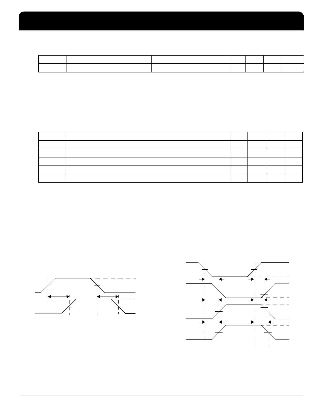
Switching Waveforms
Input
2.5V
tPLH
Output
2.5V
2.5V
3.5V
tPHL
2.5V
1.5V
VOH
VOL
Voltage Waveforms Propagation Delay Times
CTL
tPZL
Input A
tPZH
Output A
tPZH
Output A
1.25V
tPLZ
VDD/2
tPHZ
VDD/2
tPHZ
VDD/2
VDD
1.25V
0V
VDD
VOL+0.3V VOL
VOH-0.3V VOH
VDD/2
1.5V
VOH
VOL
Voltage Waveforms Enable and Disable Times
WIDE BANDWIDTH VIDEO SIGNAL SWITCH, 5 PORT
4
CONFIDENTIAL
IDTVS512
7013/7
Share Link: 