IDT72205LB10TF(2000) View Datasheet(PDF) - Integrated Device Technology
Part Name
Description
View to exact match
IDT72205LB10TF
(Rev.:2000)
(Rev.:2000)
Integrated Device Technology

IDT72205LB10TF Datasheet PDF : 16 Pages
| |||
IDT72205LB/72215LB/72225LB/72235LB/72245LB CMOS SyncFIFO™
256 x 18, 512 x 18, 1,024 x 18, 2,048 x 18 and 4,096 x 18
Commercial And Industrial Temperature Ranges
After half of the memory is filled, and at the LOW-to-HIGH
transition of the next write cycle, the Half-Full Flag goes LOW
and will remain set until the difference between the write
pointer and read pointer is less than or equal to one half of the
total memory of the device. The Half-Full Flag (HF) is then
reset to HIGH by the LOW-to-HIGH transition of the read clock
(RCLK). The HF is asynchronous.
In the Daisy Chain Depth Expansion mode, WXI is connected
to WXO of the previous device. This output acts as a signal to the
next device in the Daisy Chain by providing a pulse when the
previous device writes to the last location of memory.
READ EXPANSION OUT (RXO)
In the Daisy Chain Depth Expansion configuration, Read
Expansion In (RXI) is connected to Read Expansion Out (RXO)
of the previous device. This output acts as a signal to the next
device in the Daisy Chain by providing a pulse when the
previous device reads from the last location of memory.
DATA OUTPUTS (Q0-Q17)
Q0-Q17 are data outputs for 18-bit wide data.
,,
,
,,
Q0 - Q17
t RS
tRSS
t RSF
t RSF
t RSF
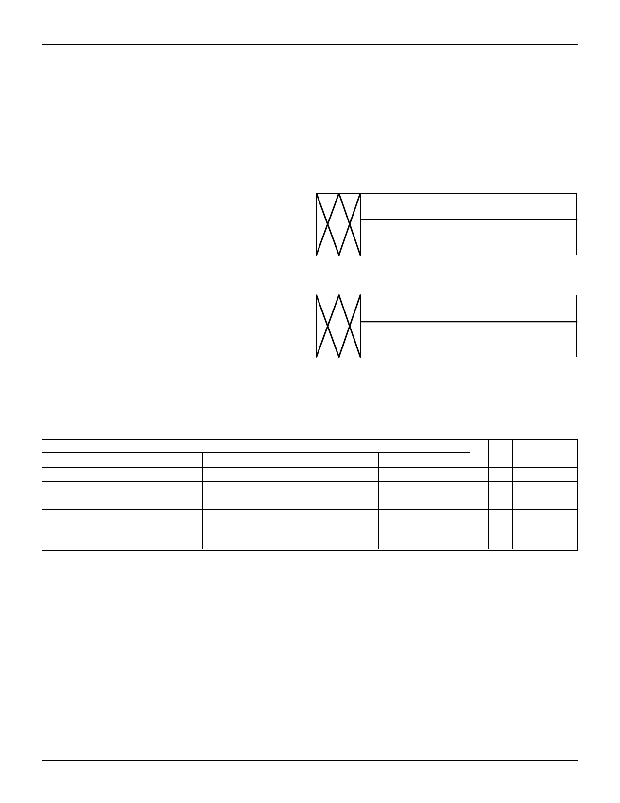
NOTES:
1. After reset, the outputs will be LOW if OE = 0 and tri-state if OE = 1.
2. The clocks (RCLK, WCLK) can be free-running during reset.
Figure 4. Reset Timing(2)
t RSR
= 1(1)
=0
2766 drw 06
8
Share Link: