HT77XX View Datasheet(PDF) - Holtek Semiconductor
Part Name
Description
View to exact match
HT77XX Datasheet PDF : 19 Pages
| |||
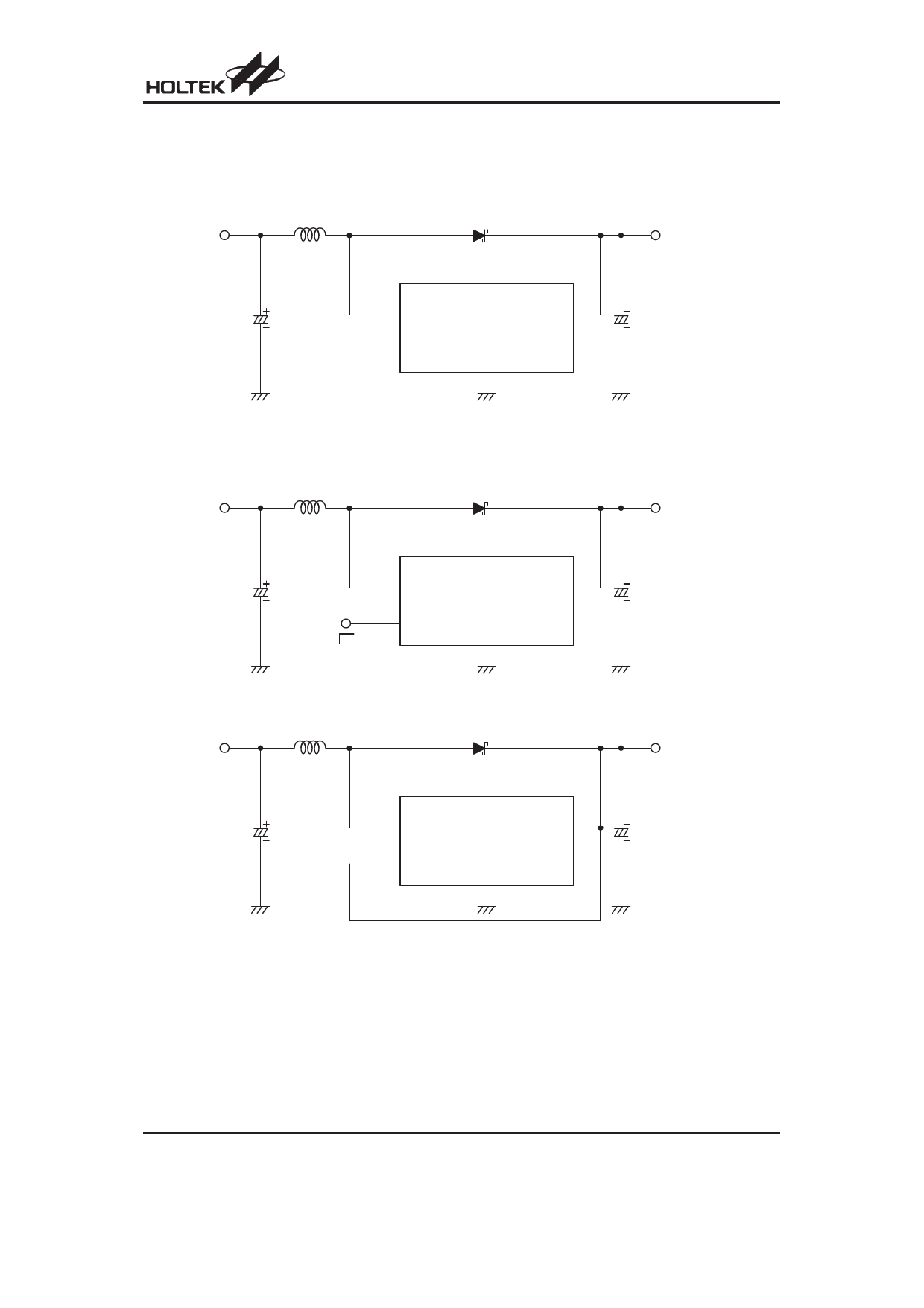
Application Circuits
Without CE Pin
G S 5 4 -1 0 1 K
G a n g S o n g E le c tr o n ic s C o ., L td .
100mH
1N 5817
V IN
HT77XX
V OUT
4 7 m F ( T a n ta lu m )
LX
H T77X X
VO UT
S e r ie s
GND
With CE Pin
V IN
G S 5 4 -1 0 1 K
G a n g S o n g E le c tr o n ic s C o ., L td .
100mH
1N 5817
1 0 0 m F ( T a n ta lu m )
V OUT
4 7 m F ( T a n ta lu m )
LX
H T77X X
VO UT
S e r ie s
CE
GND
G S 5 4 -1 0 1 K
G a n g S o n g E le c tr o n ic s C o ., L td .
100mH
1N 5817
V IN
1 0 0 m F ( T a n ta lu m )
V OUT
4 7 m F ( T a n ta lu m )
LX
H T77X X
VO UT
S e r ie s
CE
GND
1 0 0 m F ( T a n ta lu m )
Note:
For the SOT23-5 package, when CE is pulled low, the internal blocks of the device, such as the reference band
gap, gain block, and all feedback and control circuitry will be switched off. The boost converter¢s output, VOUT,
will be at a value one Schottky diode voltage drop below the input voltage and the LX pin remains in a high im-
pedance condition. The output capacitor and load at VOUT determine the rate at which VOUT decays.
Rev 1.90
10
October 13, 2010
Share Link: 