CS52015-3GST3 View Datasheet(PDF) - Cherry semiconductor
Part Name
Description
View to exact match
CS52015-3GST3 Datasheet PDF : 6 Pages
| |||
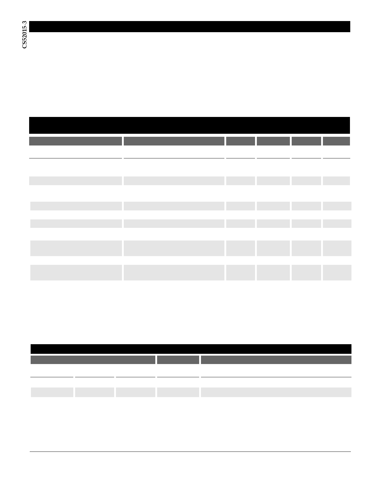
Absolute Maximum Ratings
Supply Voltage, VIN.....................................................................................................................................................................7V
Operating Temperature Range................................................................................................................................-40¡C to 70¡C
Junction Temperature ............................................................................................................................................................150¡C
Storage Temperature Range ..................................................................................................................................-60¡C to 150¡C
Lead Temperature Soldering
Wave Solder (through hole styles only) .....................................................................................10 sec. max, 260¡C peak
Reflow (SMD styles only) ......................................................................................60 sec. max above 183¡C, 230¡C peak
ESD Damage Threshold............................................................................................................................................................2kV
Electrical Characteristics: CIN = 10µF, COUT = 22µF Tantalum, VOUT + VDROPOUT < VIN < 7V, 0¡C ² TA ² 70¡C, TJ ² +150¡C,
unless otherwise specified, Ifull load = 1.5A.
PARAMETER
TEST CONDITIONS
MIN
TYP
MAX
UNIT
s Fixed Output Voltage
Output Voltage
(Notes 1 and 2)
Line Regulation
Load Regulation
(Notes 1 and 2)
Dropout Voltage (Note 3)
Current Limit
Quiescent Current
Thermal Regulation (Note 4)
Ripple Rejection
(Note 4)
Thermal Shutdown (Note 5)
Thermal Shutdown Hysteresis
(Note 5)
VINÐVOUT=1.5V
0²IOUT²1.5A
2V²VINÐVOUT²3.7V; IOUT=10mA
VINÐVOUT=2V; 10mA ²IOUT²1.5A
3.250
(-1.5%)
IOUT=1.5A
VINÐVOUT=3V
1.6
IOUT=10mA
30ms pulse; TA=25¡C
f=120Hz; IOUT=1.5A; VINÐVOUT=3V;
VRIPPLE=1VP-P
150
3.300
0.02
0.04
1.05
3.1
5.0
0.002
80
180
25
3.350
V
(+1.5%)
0.20
%
0.4
%
1.4
10.0
0.020
V
A
mA
%/W
dB
210
¡C
¡C
Note 1: Load regulation and output voltage are measured at a constant junction temperature by low duty cycle pulse testing. Changes in out-
put voltage due to temperature changes must be taken into account separately.
Note 2: Specifications apply for an external Kelvin sense connection at a point on the output pin 1/4Ó from the bottom of the package.
Note 3: Dropout voltage is a measurement of the minimum input/output differential at full load.
Note 4: Guaranteed by design, not tested in production.
Note 5: Thermal shutdown is 100% functionally tested in production.
D2PAK
1
2
3
PACKAGE PIN #
TO-220
1
2
3
SOT-223
1
2
3
Package Pin Description
PIN SYMBOL
FUNCTION
Gnd
VOUT
VIN
Ground connection
Regulated output voltage (case).
Input voltage
2
Share Link: 