HD74AC283 View Datasheet(PDF) - Renesas Electronics
Part Name
Description
View to exact match
HD74AC283 Datasheet PDF : 10 Pages
| |||
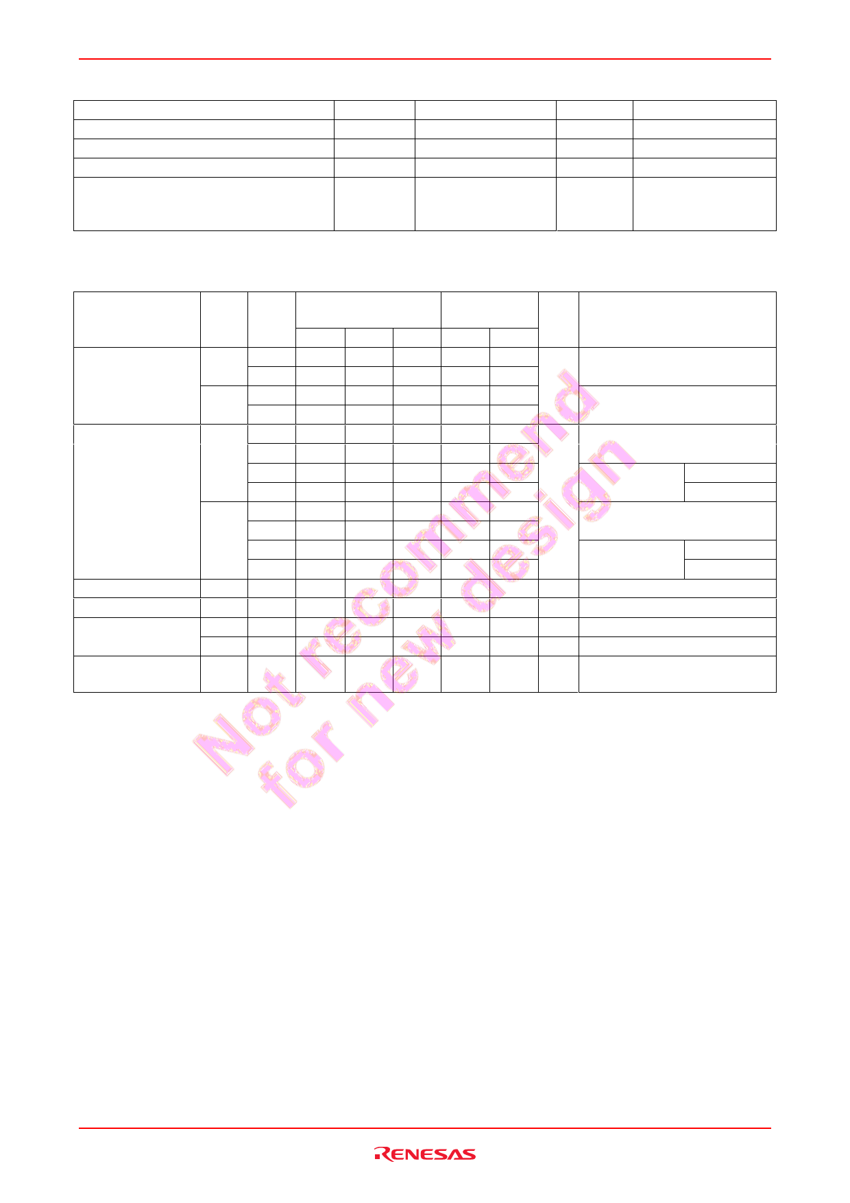
HD74AC283/HD74ACT283
Recommended Operating Conditions: HD74ACT283
Item
Supply voltage
Input and output voltage
Operating temperature
Input rise and fall time
(except Schmitt inputs)
VIN 0.8 to 2.0 V
Symbol
VCC
VI, VO
Ta
tr, tf
Ratings
2 to 6
0 to VCC
–40 to +85
8
Unit
V
V
°C
ns/V
Condition
VCC = 4.5V
VCC = 5.5V
DC Characteristics: HD74ACT283
Item
Sym- VCC
bol (V)
Ta = 25°C
min. typ. max.
Input voltage
VIH
4.5
2.0
1.5
—
5.5 2.0 1.5 —
VIL
4.5 —
5.5 —
1.5 0.8
1.5 0.8
Output voltage
VOH 4.5
4.4
4.49 —
5.5 5.4 5.49 —
4.5 3.94 —
—
5.5 4.94 —
—
VOL
4.5
—
5.5 —
0.001 0.1
0.001 0.1
4.5 —
—
0.32
5.5 —
—
0.32
Input current
IIN
5.5 —
ICC/input current
ICCT
5.5
—
Dynamic output
IOLD
5.5
—
current*
IOHD
5.5
—
Quiescent supply ICC
5.5 —
current
—
±0.1
0.6 —
—
—
—
—
—
8.0
*Maximum test duration 2.0 ms, one output loaded at a time.
Ta = –40 to
+85°C
min. max.
2.0 —
2.0 —
—
0.8
—
0.8
4.4 —
5.4 —
3.80 —
4.80 —
—
0.1
—
0.1
—
0.37
—
0.37
—
±1.0
—
1.5
86
—
–75 —
—
80
Unit
Condition
V
VOUT = 0.1 V or Vcc–0.1 V
VOUT = 0.1 V or Vcc–0.1 V
V
VIN = VIL or VIH
IOUT = –50 µA
VIN = VIL
VIN = VIL or VIH
IOUT = 50 µA
IOH = –24 mA
IOH = –24 mA
VIN = VIL
IOL = 24 mA
IOL = 24 mA
µA VIN = VCC or GND
mA VIN = VCC–2.1 V
mA VOLD = 1.1 V
mA VOHD = 3.85 V
µA VIN = VCC or ground
Rev.2.00, Jul.16.2004, page 6 of 9
Share Link: 