HEC40195BDB View Datasheet(PDF) - Philips Electronics
Part Name
Description
View to exact match
HEC40195BDB Datasheet PDF : 8 Pages
| |||
Philips Semiconductors
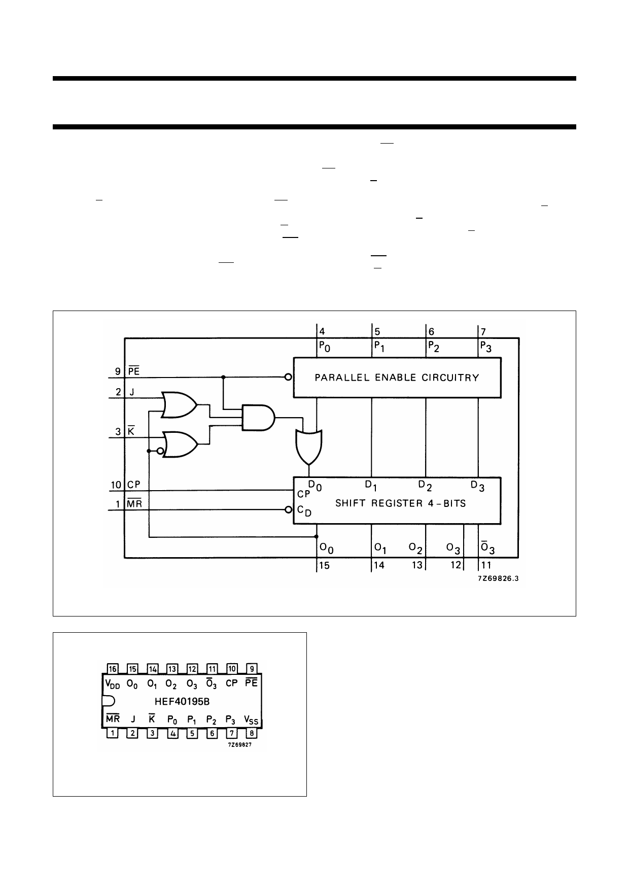
4-bit universal shift register
Product specification
HEF40195B
MSI
DESCRIPTION
The HEF40195B is a fully synchronous edge-triggered
4-bit shift register with a clock input (CP), four synchronous
parallel data inputs (P0 to P3), two synchronous serial data
inputs (J, K), a synchronous parallel enable input (PE),
buffered parallel outputs from all 4-bit positions (O0 to O3),
a buffered inverted output from the last bit position (O3)
and an overriding asynchronous master reset input (MR).
Each register stage is of a D-type master-slave flip-flop.
Operation is synchronous (except for MR) and is
edge-triggered on the LOW to HIGH transition of the CP
input. When PE is LOW, data are loaded into the register
from P0 to P3 on the LOW to HIGH transition of CP. When
PE is HIGH, data are shifted into the first register position
from J and K and all the data in the register are shifted one
position to the right on the LOW to HIGH transition of CP.
D-type entry is obtained by interconnecting J and K.
When J is HIGH and K is LOW, the first stage is in the
toggle mode. When J is LOW and K is HIGH, the first stage
is in the hold mode.
A LOW on MR resets all four bit positions (O0 to
O3 = LOW, O3 = HIGH) independent of all other input
conditions.
Fig.1 Functional diagram.
Fig.2 Pinning diagram.
January 1995
HEF40195BP(N): 16-lead DIL; plastic
(SOT38-1)
HEF40195BD(F): 16-lead DIL; ceramic (cerdip)
(SOT74)
HEF40195BT(D): 16-lead SO; plastic
(SOT109-1)
( ): Package Designator North America
FAMILY DATA, IDD LIMITS category MSI
See Family Specifications
2
Share Link: 