HEC40194BN View Datasheet(PDF) - Philips Electronics
Part Name
Description
View to exact match
HEC40194BN Datasheet PDF : 8 Pages
| |||
Philips Semiconductors
4-bit bidirectional universal shift register
Product specification
HEF40194B
MSI
DESCRIPTION
The HEF40194B is a 4-bit bidirectional shift register with
two mode control inputs (S0 and S1), a clock input (CP), a
serial data shift left input (DSL), a serial data shift right input
(DSR), four parallel data inputs (P0 to P3), an overriding
asynchronous master reset input (MR), and four buffered
parallel outputs (O0 to O3). When LOW, MR resets all
stages and forces O0 to O3 LOW, overriding all other input
conditions. When MR is HIGH, the operation mode is
controlled by S0 and S1 as shown in the function table.
Serial and parallel operation are edge-triggered on the
LOW to HIGH transition of CP. The inputs at which the
data are to be entered and S0, S1 must be stable for a
set-up time before the LOW to HIGH transition of CP.
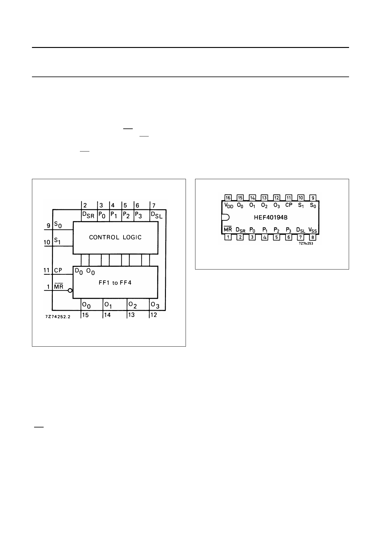
Fig.2 Pinning diagram.
Fig.1 Functional diagram.
HEF40194BP(N): 16-lead DIL; plastic
(SOT38-1)
HEF40194BD(F): 16-lead DIL; ceramic (cerdip)
(SOT74)
HEF40194BT(D): 16-lead SO; plastic
(SOT109-1)
( ): Package Designator North America
PINNING
S0, S1
P0 to P3
DSR
DSL
CP
MR
O0 to O3
mode control inputs
parallel data inputs
serial data shift right input
serial data shift left input
clock input (LOW to HIGH edge-triggered)
master reset input (active LOW)
buffered parallel outputs
FAMILY DATA, IDD LIMITS category MSI
See Family Specifications
January 1995
2
Share Link: 