CS8120 View Datasheet(PDF) - Cherry semiconductor
Part Name
Description
View to exact match
CS8120 Datasheet PDF : 8 Pages
| |||
Absolute Maximum Ratings
DC Input Voltage ...........................................................................................................................................................-0.7 to 26V
Load Dump .................................................................................................................................................................................60V
Output Current .................................................................................................................................................Internally Limited
Electrostatic Discharge (Human Body Model) ......................................................................................................................2kV
Operating Temperature .......................................................................................................................................-40¡C to +125¡C
Junction Temperature...........................................................................................................................................-40¡C to +150¡C
Storage Temperature ............................................................................................................................................-55¡C to +150¡C
Lead Temperature Soldering
Wave Solder (through hole styles only) .....................................................................................10 sec. max, 260¡C peak
Reflow (SMD styles only) ......................................................................................60 sec. max above 183¡C, 230¡C peak
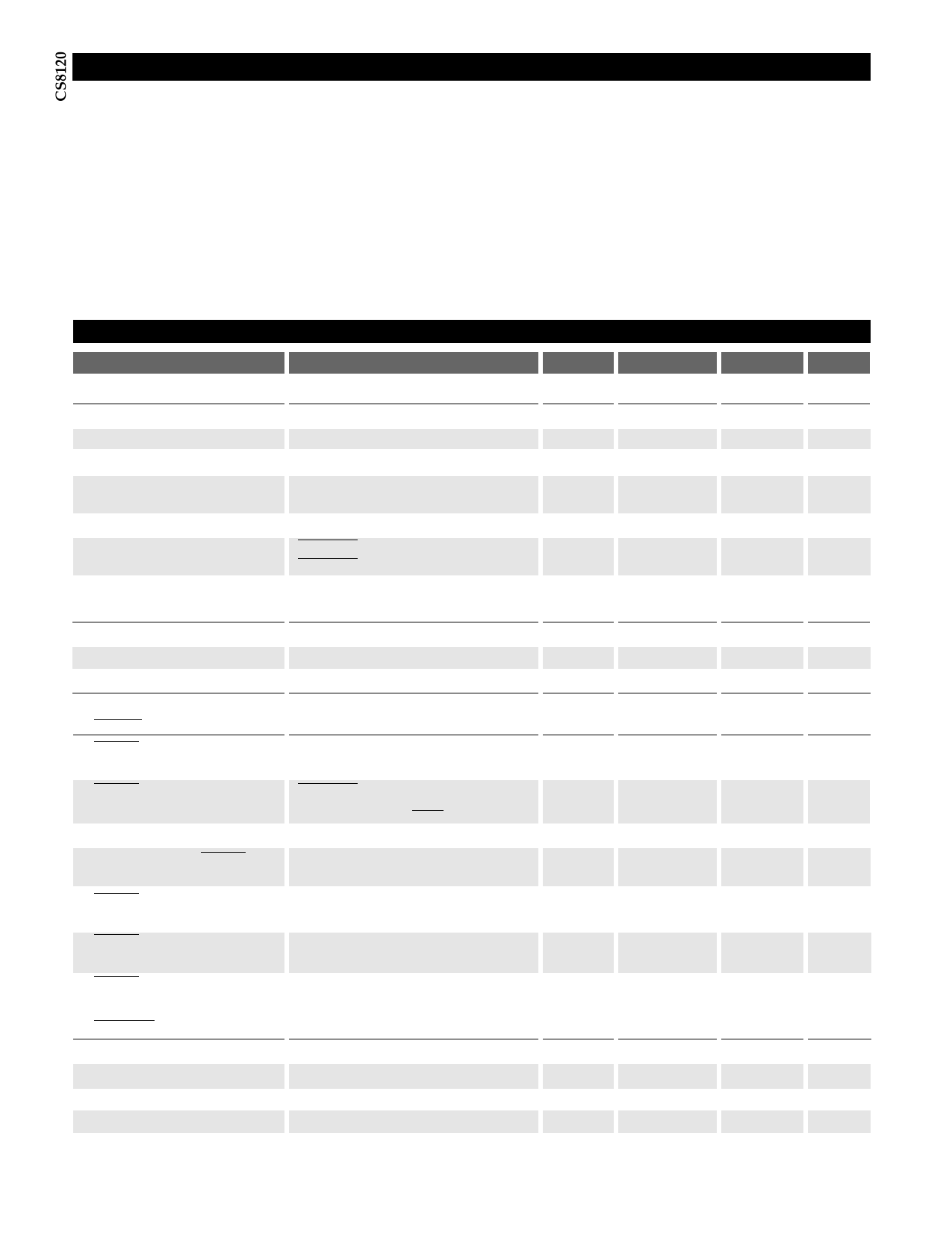
Electrical Characteristics:
V
IN
=
14V,
I
OUT
=5
mA,
-40ûC
²
TJ
²
150ûC,
-40ûC
²
TC ² 125ûC unless otherwise specified
PARAMETER
TEST CONDITIONS
MIN
TYP
MAX
UNIT
s Output Stage
Output Voltage, VOUT
7V ² VIN ² 26V, 1mA ² IOUT ² 300mA 4.8
5.0
Line Regulation
7V ² VIN ² 26V, IOUT = 200mA
Load Regulation
1mA ² IOUT ² 300mA
Supply Voltage Rejection
VIN = 14VDC + 1VRMS
@120Hz, ILOAD = 25½
40
70
Dropout Voltage
IOUT = 200mA
1.0
Quiescent Current
ENABLE = High, VIN = 12V
0.25
ENABLE = Low, IOUT = 200mA
2.5
5.2
V
50
mV
50
mV
dB
1.5
V
0.65
mA
15.0
mA
s Protection Circuits
Short Circuit Current
Thermal Shutdown
Overvoltage Shutdown
300
600
mA
150
190
ûC
26
40
V
s RESET
RESET Saturation Voltage
RESET Output Leakage
Current
1V < VOUT < VRT(OFF), 3.1k½ pull-up
to VOUT
ENABLE = Low
VOUT > VRT(ON), V RESET = VOUT
0.1
0.4
V
0
25
µA
Power ON/OFF RESET
Peak Output Voltage
RESET Threshold ON
(VOUT Increasing)
RESET Threshold OFF
(VOUT Decreasing)
RESET Threshold Hysteresis
3.1k½ pull-up to VOUT
0.7
1.0
V
VOUT - 0.10 VOUT - 0.04 V
4.75
VOUT - 0.14
V
10
40
mV
s ENABLE
Input High Voltage
Input Low Voltage
Input Hysteresis
Input Current
7V < VIN < 26V
7V < VIN < 26V
7V < VIN < 26V
Gnd < VIN(HI) < VOUT
2.9
1.1
2.1
0.4
0.8
-10
0
3.9
V
V
2.8
V
+10
µA
* To have safe operating junction temperatures, low duty cycle pulse testing is used on tests where applicable.
2
Share Link: 