CS51411 View Datasheet(PDF) - ON Semiconductor
Part Name
Description
View to exact match
CS51411 Datasheet PDF : 20 Pages
| |||
CS51411, CS51412, CS51413, CS51414
Control Ramp Generation
In original V2 designs, the control ramp VCR was
generated from the converter's output ripple. Using a current
derived ramp provides the same benefits as current mode,
namely input feed forward, single pole output filter
compensation and fast feedback following output load
transients. Typically a tantalum or organic polymer
capacitor is selected having a sufficiently large ESR
component, relative to its capacitive and ESL ripple
contributions, to ensure the control ramp was sensing
inductor current and its amplitude was sufficient to maintain
loop stability. This technique is illustrated in Figure 6.
VIN
VOUT
L
Cesr
C
VIN
RC
VOUT
VFB
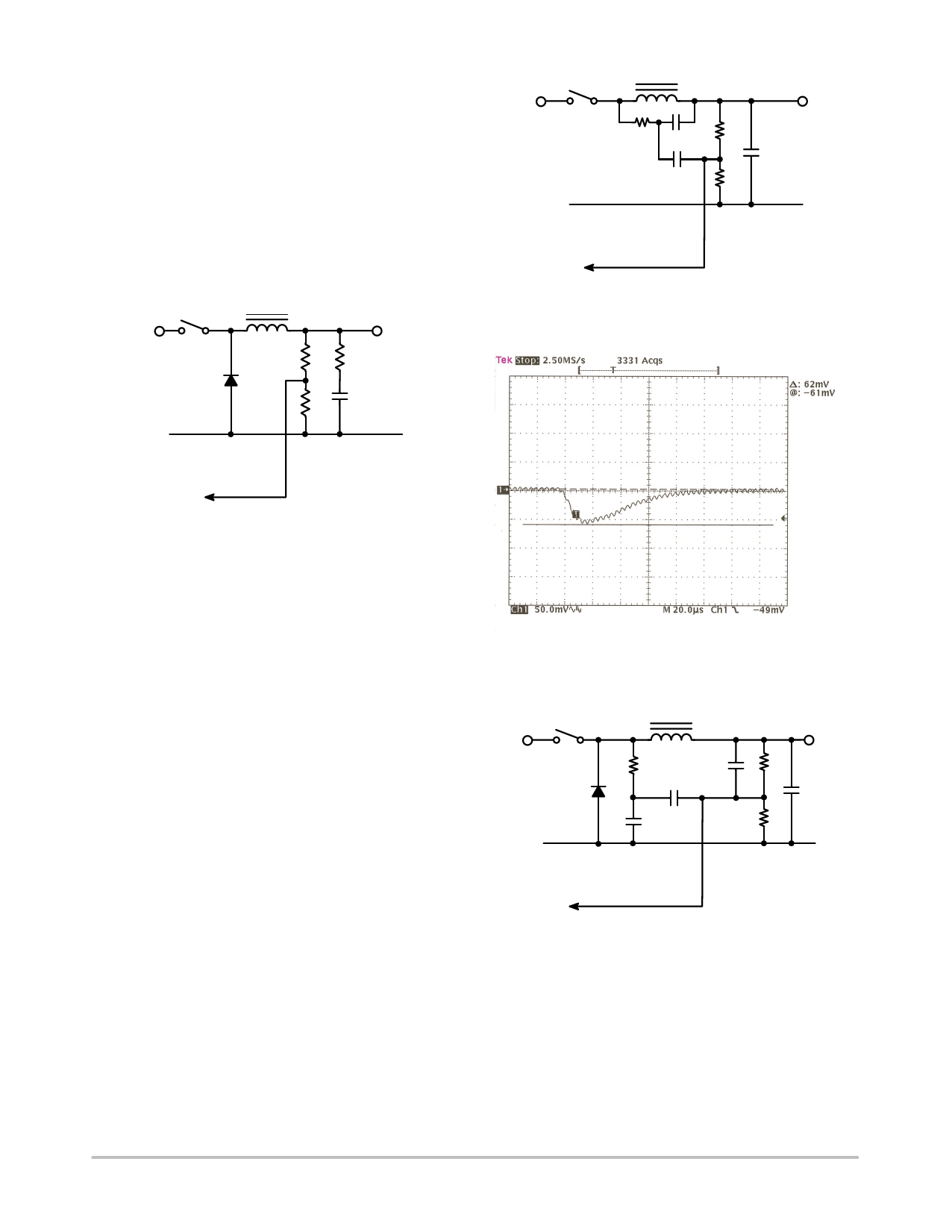
Figure 7. Control Ramp Generated from DCR
Inductor Sensing
VFB
Figure 6. Control Ramp Generated from Output
Advances in multilayer ceramic capacitor technology are
such that MLCC's can provide a cost effective filter solution
for low voltage (< 12 V), high frequency converters
(>200 kHz). For example, a 10 mF MLCC 16 V in a
805 SMT package has an ESR of 2 mW and an ESL of
100 nH. Using several MLCC's in parallel, connected to
power and ground planes on a PCB with multiple vias, can
provide a “near perfect” capacitor. Using this technique,
output switching ripple below 10 mV can be readily
obtained since parasitic ESR and ESL ripple contributions
are nil. In this case, the control ramp is generated elsewhere
in the circuit.
Ramp generation using dcr inductor current sensing,
where the L/DCR time constant of the output inductor is
matched with the CR time constant of the integrating
network, is shown in Figure 7. The converter's transient
response following a 1 A step load is shown in Figure 8. This
transient response is indicative of a closed loop in excess of
10 kHz having good gain and phase margin in the frequency
domain. Also note the amplitude of output switching ripple
provided by just two 10 mF MLCC's.
Figure 8.
Ramp generation using a voltage feed forward technique
is illustrated in Figure 9.
VIN
VOUT
Rf
CZ
Cf
VFB
Figure 9. Control Ramp from Voltage Feed Forward
http://onsemi.com
8
Share Link: 