BD3021HFP-M(2009) View Datasheet(PDF) - ROHM Semiconductor
Part Name
Description
View to exact match
BD3021HFP-M Datasheet PDF : 5 Pages
| |||
4/4
7. Testing on application boards
When testing the IC on an application board, connecting a capacitor directly to a low-impedance pin may subject the IC to stress. Always
discharge capacitors completely after each process or step. The IC’s power supply should always be turned off completely before
connecting or removing it from a jig or fixture during the evaluation process. To prevent damage from static discharge, ground the IC during
assembly and use similar precautions during transport and storage.
8. Thermal consideration
Use a thermal design that allows for a sufficient margin in light of the Pd in actual operating conditions.
Consider Pc that does not exceed Pd in actual operating conditions. (Pd≧Pc)
Tjmax : Maximum junction temperature=150℃, Ta : Peripheral temperature[℃] ,
θja : Thermal resistance of package-ambience[℃/W], Pd : Package Power dissipation [W],
Pc : Power dissipation [W], Vcc : Input Voltage, VOUT : Output Voltage, Io : Load, Icc2 : Bias Current2
Package Power dissipation : Pd (W)=(Tjmax-Ta)/θja
Power dissipation
: Pc (W)=(Vcc-VOUT)×Io+Vcc×Icc2
9. Over current protection circuit (OCP)
The IC incorporates an integrated over-current protection circuit that operates in accordance with the rated output capacity. This circuit
serves to protect the IC from damage when the load becomes shorted. It is also designed to limit output current (without latching) in the
event of a large and instantaneous current flow from a large capacitor or other component. These protection circuits are effective in
preventing damage due to sudden and unexpected accidents. However, the IC should not be used in applications characterized by the
continuous or transitive operation of the protection circuits.
10. Thermal shutdown circuit (TSD)
The IC incorporates a built-in thermal shutdown circuit, which is designed to turn the IC off completely in the event of thermal overload. It is
not designed to protect the IC from damage or guarantee its operation. ICs should not be used after this function has activated, or in
applications where the operation of this circuit is assumed.
11. Applications or inspection processes where the potential of the Vcc pin or other pins may be reversed from their normal state may
cause damage to the IC's internal circuitry or elements. Use an output pin capacitance of 1000μF or lower in case Vcc is shorted with the
GND pin while the external capacitor is charged. Insert a diode in series with Vcc to prevent reverse current flow, or insert bypass diodes
between Vcc and each pin.
12. Positive voltage surges on VCC pin
A power zener diode should be inserted between VCC and GND for protection against voltage surges of more than 50V on the VCC pin.
13. Negative voltage surges on VCC pin
A schottky barrier diode should be inserted between VCC and GND for protection against voltages lower than GND on the VCC pin.
14. Output protection diode
Loads with large inductance components may cause reverse current flow during startup or shutdown. In such cases, a protection diode
should be inserted on the output to protect the IC.
15. Regarding input pins of the IC
This monolithic IC contains P+ isolation and P substrate layers between adjacent elements in order to keep them isolated. PN junctions are
formed at the intersection of these P layers with the N layers of other elements, creating parasitic diodes and/or transistors.
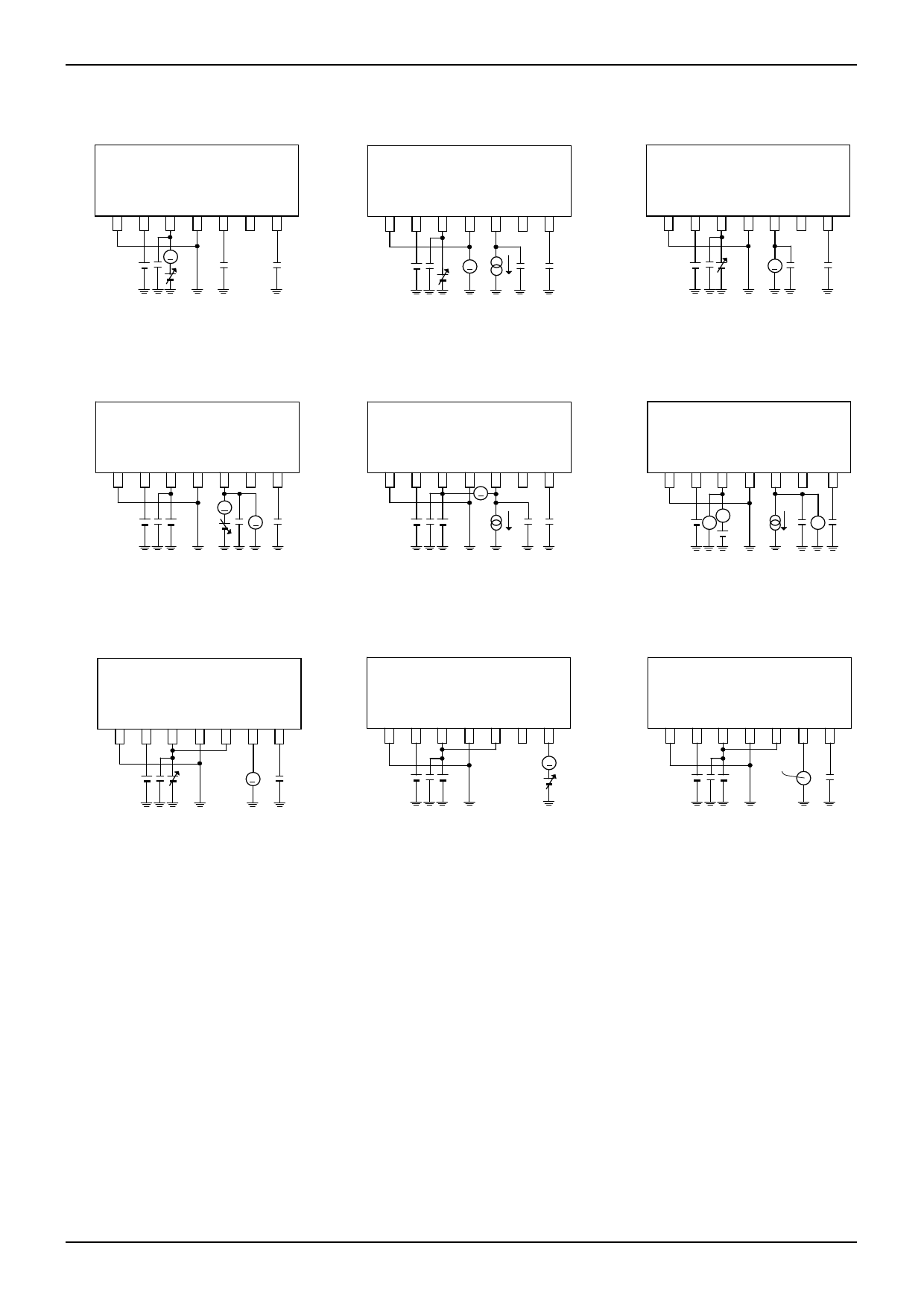
For example (refer to the figure below):
●When GND > Pin A and GND > Pin B, the PN junction operates as a parasitic diode
●When GND > Pin B, the PN junction operates as a parasitic transistor
Parasitic diodes occur inevitably in the structure of the IC, and the operation of these parasitic diodes can result in mutual interference
among circuits, operational faults, or physical damage. Accordingly, conditions that cause these diodes to operate, such as applying a
voltage lower than the GND voltage to an input pin (and thus to the P substrate) should be avoided.
(Pin A)
Resistor
(Pin B)
Transistor (NPN)
B
C
E
P+
N
P
P
N
P+
N
Parasitic elements
GND
P+
N
N
P
P+
N
N
P substrate
Parasitic elements
or transistors
GND
Example of Simple Monolithic IC Architecture
(Pin B)
BC
E
GND
Parasitic elements
or transistors
(Pin A)
Parasitic elements
REV. B
Share Link: 