AT27C520 View Datasheet(PDF) - Atmel Corporation
Part Name
Description
View to exact match
AT27C520 Datasheet PDF : 10 Pages
| |||
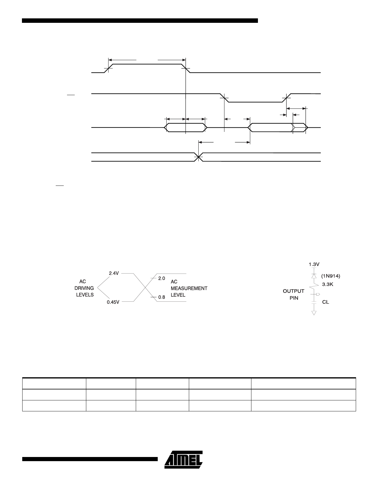
AC Waveforms for Read Operation(1)
tALE
ALE
AT27C520
OE/VPP
AD7 - AD0
tDF
tOH
tAS
tAH tOE
ADDRESS IN
DATA OUT
tACC
A15 - A8
Notes: 1. Timing measurement reference levels for all speed grades are VOL = 0.8V and VOH = 2.0V. Input AC drive levels are VIL =
0.45V and VIH = 2.4V.
2. OE/VPP may be delayed up to tACC - tOE after the address is valid without impact on tACC.
3. This parameter is only sampled and is not 100% tested.
4. Output float is defined as the point when data is no longer driven.
Input Test Waveforms and Measurement Levels
For -70 and -90 devices:
Output Test Load
tR, tF < 20 ns (10% to 90%)
Note: CL = 100 pF including jig
capacitance.
Pin Capacitance (f = 1 MHz, T = 25°C)(1)
Typ
Max
Units
Conditions
CIN
4
6
pF
VIN = 0V
COUT
8
12
pF
VOUT = 0V
Note: 1. Typical values for nominal supply voltage. This parameter is only sampled and is not 100% tested.
5
Share Link: 