AT27C516(2008) View Datasheet(PDF) - Atmel Corporation
Part Name
Description
View to exact match
AT27C516 Datasheet PDF : 13 Pages
| |||
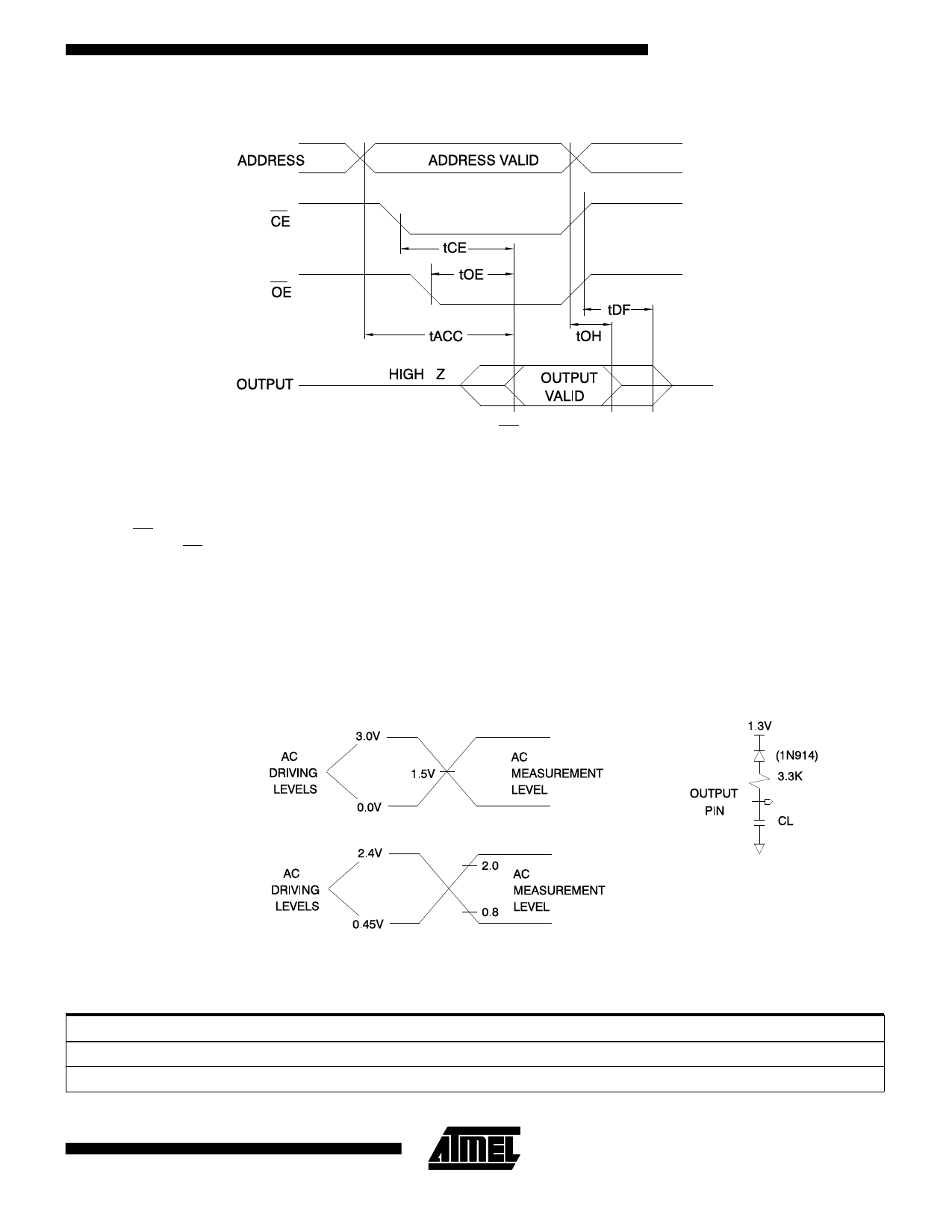
9. AC Waveforms for Read Operation(1)
AT27C516
10. AC Characteristics for Read Operation
AT27C516
-45
-70
Symbol
Parameter
Condition
Min
Max
Min
Max
Units
tACC(3)
Address to Output Delay
CE = OE = VIL
45
tCE(2)
CE to Output Delay
OE = VIL
45
tOE(2)(3)
OE to Output Delay
CE = VIL
20
tDF(4)(5)
OE or CE High to Output Float, whichever occurred first
20
70
ns
70
ns
25
ns
25
ns
tOH
Output Hold from Address, CE or OE, Whichever
Occurred First
7
7
ns
Notes:
1. Timing measurement reference level is 1.5V for -45 devices. Input AC drive levels are VIL = 0.0V and VIH = 3.0V. Timing mea-
surement reference levels for all other speed grades are VOL = 0.8V and VOH = 2.0V. Input AC drive levels are VIL = 0.45V
and VIH = 2.4V.
2. OE may be delayed up to tCE - tOE after the falling edge of CE without impact on tCE.
3. OE may be delayed up to tACC - tOE after the address is valid without impact on tACC.
4. This parameter is only sampled and is not 100% tested.
5. Output float is defined as the point when data is no longer driven.
5
0362E–EPROM–1/08
Share Link: 