AT27BV512(2007) View Datasheet(PDF) - Atmel Corporation
Part Name
Description
View to exact match
AT27BV512
(Rev.:2007)
(Rev.:2007)
Atmel Corporation

AT27BV512 Datasheet PDF : 15 Pages
| |||
AT27BV512
3. System Considerations
Switching between active and standby conditions via the Chip Enable pin may produce tran-
sient voltage excursions. Unless accommodated by the system design, these transients may
exceed datasheet limits, resulting in device non-conformance. At a minimum, a 0.1 µF high
frequency, low inherent inductance, ceramic capacitor should be utilized for each device. This
capacitor should be connected between the VCC and Ground terminals of the device, as close
to the device as possible. Additionally, to stabilize the supply voltage level on printed circuit
boards with large EPROM arrays, a 4.7 µF bulk electrolytic capacitor should be utilized, again
connected between the VCC and Ground terminals. This capacitor should be positioned as
close as possible to the point where the power supply is connected to the array.
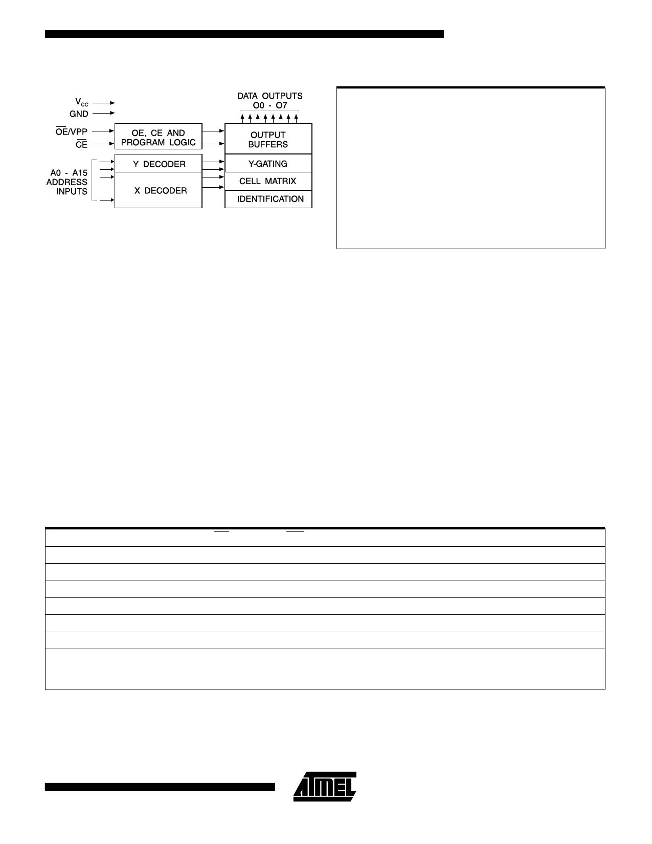
4. Block Diagram
5. Absolute Maximum Ratings*
Temperature Under Bias.................................. -40°C to +85°C
Storage Temperature ..................................... -65°C to +125°C
Voltage on Any Pin with
Respect to Ground .........................................-2.0V to +7.0V(1)
Voltage on A9 with
Respect to Ground ......................................-2.0V to +14.0V(1)
*NOTICE:
Stresses beyond those listed under “Absolute
Maximum Ratings” may cause permanent dam-
age to the device. This is a stress rating only and
functional operation of the device at these or any
other conditions beyond those indicated in the
operational sections of this specification is not
implied. Exposure to absolute maximum rating
conditions for extended periods may affect
device reliability
VPP Supply Voltage with
Respect to Ground .......................................-2.0V to +14.0V(1)
Notes: 1. Minimum voltage is -0.6V DC which may undershoot to -2.0V for pulses of less than 20 ns. Maximum output pin voltage is
VCC + 0.75V DC which may be exceeded if certain precautions are observed (consult application notes) and which may
overshoot to +7.0V for pulses of less than 20 ns.
3
0602E–EPROM–12/07
Share Link: