A1374 View Datasheet(PDF) - Allegro MicroSystems
Part Name
Description
View to exact match
A1374 Datasheet PDF : 22 Pages
| |||
A1373 and A1374
High Precision, Output Pin Programmable
Linear Hall Effect Sensors
Features and Benefits
▪ Output pin programming
▪ Field-programmable for optimal application integration
▪ Selectable coarse and fine gain and quiescent output voltage
▪ Selectable sensitivity temperature coefficient
▪ Selectable output clamp voltage level, including no-
clamp (rail-to-rail)
▪ Selectable output polarity
▪ Unipolar or bipolar operation
▪ Ratiometric sensitivity, clamps, and quiescent output voltage
▪ Chopper-stabilized Hall technique
▪ Wide operating temperature range
▪ On-chip regulator for over/under voltage protection
▪ On-chip regulator provides EMI robustness
▪ Wide lead-spacing with KB package
Package: 3 pin SIP (suffix KB)
Description
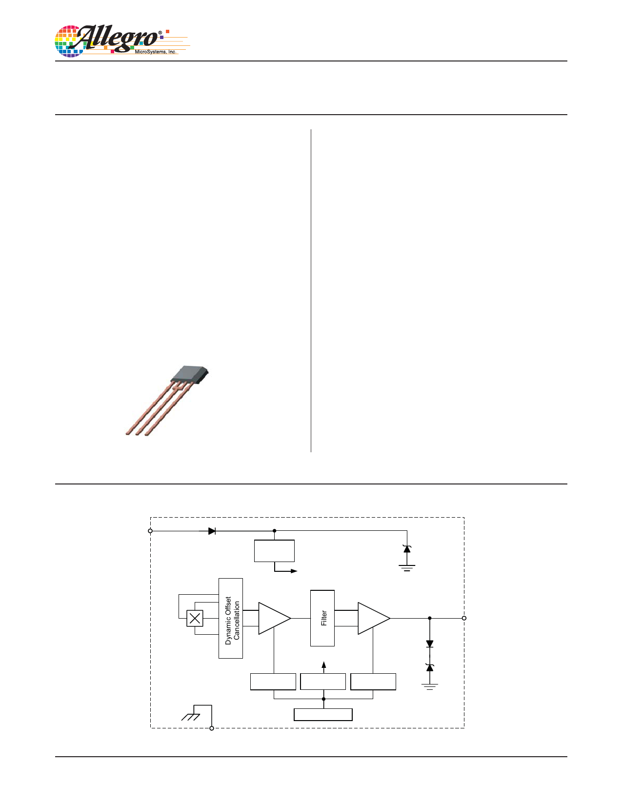
The A1373 and A1374 high precision linear Hall effect sensors
are sensitive, temperature stable, linear devices with externally
programmable features. This device family incorporates a
chopper-stabilized amplifier, voltage regulator, programming
logic, and an output amplifier on a single IC. The patented
dynamic offset cancellation used with a chopper-stabilization
technique provides extremely low offset and minimal
temperature drift.Ahigh frequency clock is used for chopping, to
ensure high frequency signal processing capability. The A1373
and A1374 are ideal for use in automotive and industrial linear
position-sensing applications that require increased reliability
and accuracy over conventional contacting-potentiometer
solutions. Key applications include: throttle position sensors,
pedal position sensors, and suspension height sensors.
The design and manufacturing flexibility of the A1373 and
A1374 complement the Allegro linear Hall effect family of
devices by offering programmable gain, quiescent offset voltage
for unipolar or bipolar operation, temperature coefficient,
clamps, and polarity. The device can be set up in a magnetic
circuit and programmed with a train of serial pulses via the
output pin. Once the right combination of gain, quiescent
Not to scale
VCC
Pin 1
Continued on the next page…
Functional Block Diagram
Voltage
Regulator
To all subcircuits
A1373-DS, Rev. 8
Amp
Out
GND
Pin 2
Gain
Hall drive circuit
Temperature
Coefficient
Offset
Trim Control
VOUT
Pin 3
Share Link: 