10XSC425 View Datasheet(PDF) - Freescale Semiconductor
Part Name
Description
View to exact match
10XSC425 Datasheet PDF : 56 Pages
| |||
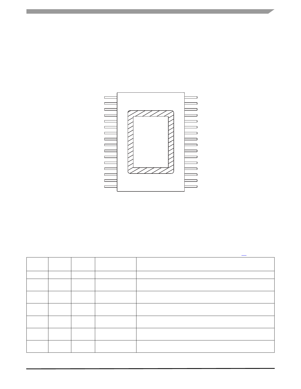
3 Pin Connections
3.1 Pinout Diagram
Transparent Top View of Package
WAKE
1
RSTB
2
CSB
3
SCLK
4
SI
5
VDD
6
SO
7
GND
8
VPWR
9
HS3
10
HS3
11
HS3
12
HS3
13
HS1
14
HS1
15
HS1
16
32
FSB
31
IN3
30
IN2
29
IN1
28
IN0
27
CSNS
26
FSI
25
GND
24
NC
23
HS2
22
HS2
21
HS2
20
HS2
19
HS0
18
HS0
17
HS0
Figure 3. 10XSC425 Pin Connections
3.2 Pin Definitions
Table 2. 10XSC425 Pin Definitions
A functional description of each pin can be found in the Functional Pin Description section beginning on page 28.
Pin
Number
Pin Name
Pin
Function
Formal Name
Definition
1
WAKE
Input
2
RSTB
Input
Wake
Reset
This input pin controls the device mode.
This input pin is used to initialize the device configuration and fault registers,
as well as drive the device into a low-current Sleep mode.
3
CSB
Input
4
SCLK
Input
Chip Select
(Active Low)
Serial Clock
This input pin is connected to a chip select output of a master microcontroller
(MCU).
This input pin is connected to the MCU providing the required bit shift clock for
SPI communication.
5
SI
Input
Serial Input
This pin is a command data input pin connected to the SPI Serial Data Output
of the MCU or to the SO pin of the previous device of a daisy-chain of devices.
6
VDD
Power Digital Drain Voltage This pin is an external voltage input pin used to supply power interfaces to the
SPI bus.
7
SO
Output
Serial Output
This output pin is connected to the SPI Serial Data Input pin of the MCU or to
the SI pin of the next device of a daisy-chain of devices.
Analog Integrated Circuit Device Data
Freescale Semiconductor
10XSC425
7
Share Link: 