RT9568(2001) View Datasheet(PDF) - Richtek Technology
Part Name
Description
View to exact match
RT9568 Datasheet PDF : 6 Pages
| |||
RT9568
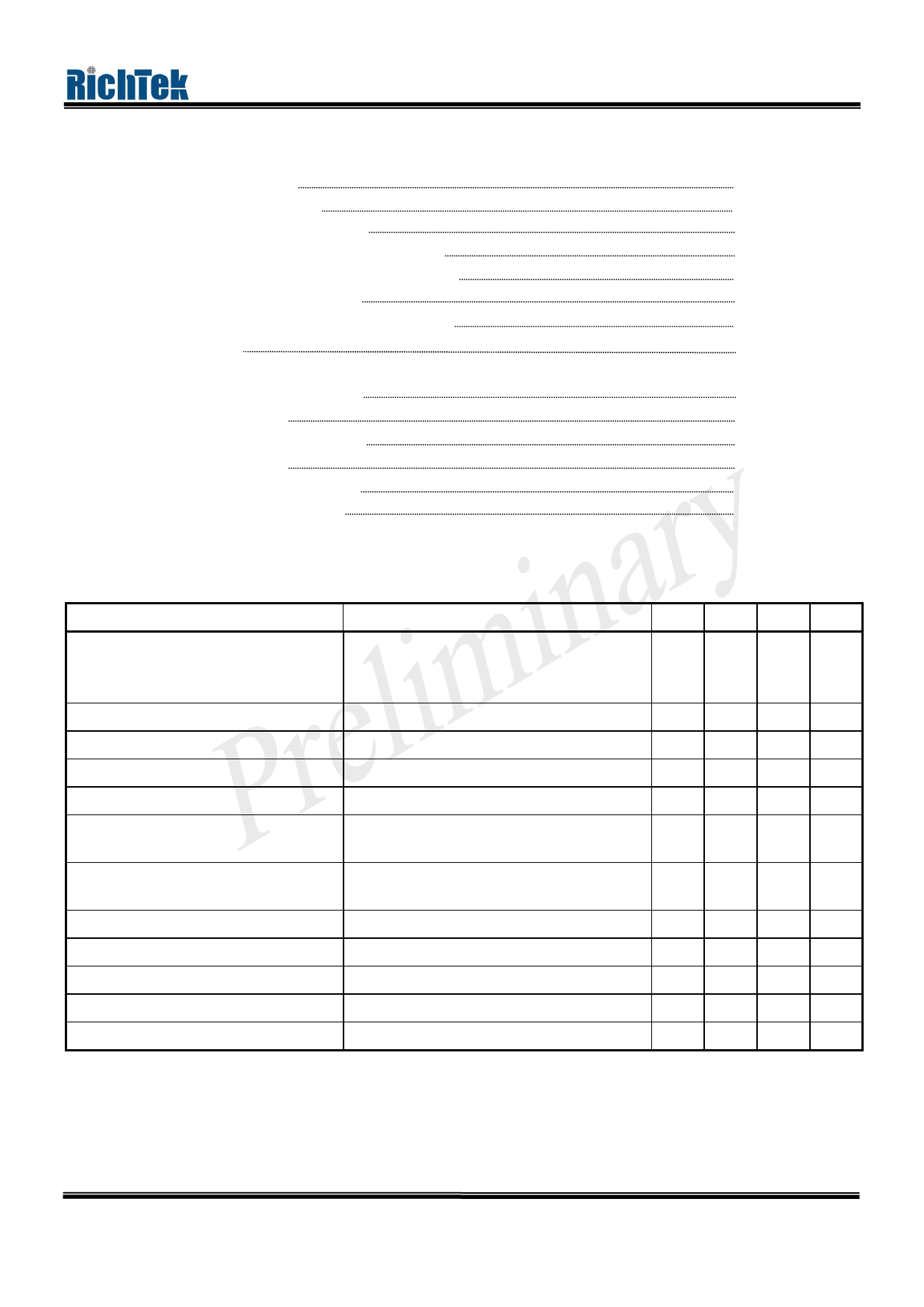
Absolute Maximum Ratings
• Power Supply Voltage
• Feedback Input Voltage Range
• Switch Collector Voltage
• Switch Emitter Voltage(VPIN8 = 30V)
• Switch Collector to Emitter Voltage
• Driver Collector Voltage
• Driver Collector Current (see Note 1)
• Switch Current
• Power Dissipation, PD @ TA = 25°C
DIP-8
SOP-8
• Package Thermal Resistance
DIP-8, θJA
SOP-8, θJA
• Operating Junction Temperature Range
• Storage Temperature Range
Note: 1.Maximum package power dissipation limits must be observed.
30V
0.3V to Vcc
30V
30V
30V
30V
100mA
1.5A
1.25W
0.625W
100°C/W
160°C/W
-40 ~ 125°C
-65 ~ 150°C
Electrical Characteristics
(VCC = 5V, TA = 25°C, unless otherwise specified)
Parameter
Symbol
Test Conditions
Min Typ Max Units
Supply Current
Current Limit Sense Voltage
Charge Current
Discharge Current
Discharge to Charge Current Ratio
VCC = 5.0V to 30V,
ICC
CT = 1.0nF, Pin6 = VCC,
--
Vpin4 > Vref, Pin1 = GND,
3.0 4.5 mA
Remaining pins open
VLIMIT
ICHG
IDISCHG
ICHG = IDISCHG
5.0V ≤ VCC ≤ 30V
5.0V ≤ VCC ≤ 30V
Pin6 to VCC
280 330 380 mV
25
36
43 µA
160 250 290 µA
5.5 6.9 7.9
--
Saturation Voltage, Darlington Connection
ISW = 1.0A, Pins 7,8
connected
--
1.0 1.3
V
Saturation Voltage, Darlington Connection
DC Current Gain
Collector Off-state Current
Reference Voltage
Reference Voltage Line Regulation
Input Bias Current
VREF
IBIAS
ISW = 1.0A,
RPIN7 = 82Ω to VCC
Forced β ≅ 20
ISW = 1.0A, VCE = 5.0V
VCE = 30V
3.0V ≤ VCC ≤ 30V
VIN = 0V
--
0.5 0.7
V
50
75
--
--
-- 0.01 100 µA
1.225 1.25 1.275 V
--
1.4 5.0 mV
--
-20 -400 nA
www.richtek-ic.com.tw
2
DS9568-02 May 2001
Share Link: 