MC74VHCT373A(2011) View Datasheet(PDF) - ON Semiconductor
Part Name
Description
View to exact match
MC74VHCT373A Datasheet PDF : 7 Pages
| |||
MC74VHCT373A
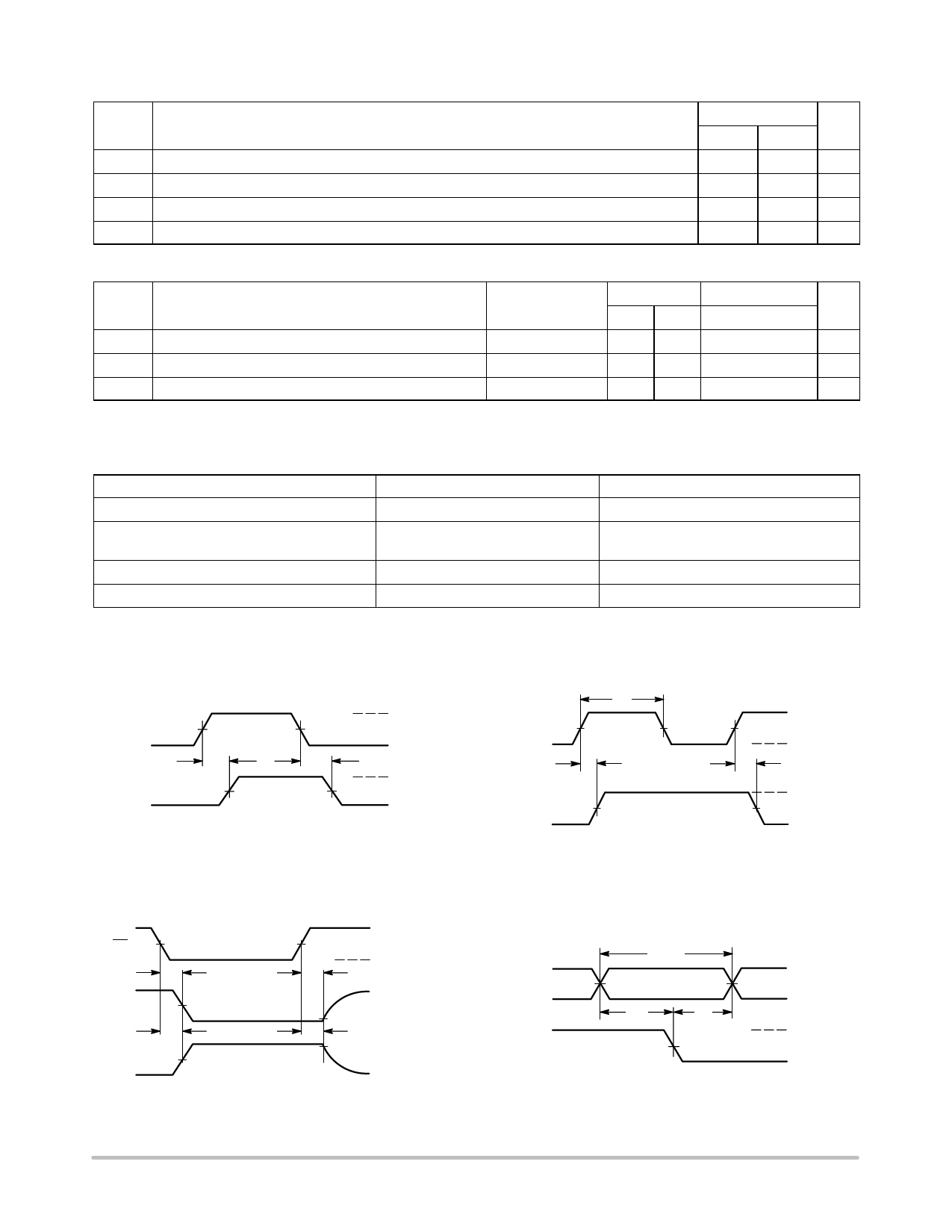
NOISE CHARACTERISTICS (Input tr = tf = 3.0ns, CL = 50 pF, VCC = 5.0V)
Symbol
Parameter
VOLP Quiet Output Maximum Dynamic VOL
VOLV Quiet Output Minimum Dynamic VOL
VIHD Minimum High Level Dynamic Input Voltage
VILD Maximum Low Level Dynamic Input Voltage
TA = 25°C
Typ
Max
Unit
1.2
1.6
V
−1.2
−1.6
V
2.0
V
0.8
V
TIMING REQUIREMENTS (Input tr = tf = 3.0ns)
Symbol
Parameter
tw(h) Minimum Pulse Width, LE
tsu Minimum Setup Time, D to LE
th
Minimum Hold Time, D to LE
Test Conditions
VCC = 5.0 ±0.5 V
VCC = 5.0 ± 0.5 V
VCC = 5.0 ± 0.5 V
TA = 25°C TA = − 40 to 85°C
Typ Limit
Limit
Unit
6.5
8.5
ns
1.5
1.5
ns
3.5
3.5
ns
ORDERING INFORMATION
Device
MC74VHCT373ADWRG
Package
SOIC−20WB
(Pb−Free)
Shipping†
1000 / Tape & Reel
MC74VHCT373ADTRG
TSSOP−20*
2500 / Tape & Reel
†For information on tape and reel specifications, including part orientation and tape sizes, please refer to our Tape and Reel Packaging
Specifications Brochure, BRD8011/D.
*This package is inherently Pb−Free.
D
tPLH
Q
1.5V
1.5V
3V
GND
tPHL
VOH
VOL
Figure 3. Switching Waveform
tw
3V
LE
1.5V
GND
tPLH
tPHL
VOH
Q
1.5V
VOL
Figure 4. Switching Waveform
OE
1.5V
tPZL
tPLZ
Q
1.5V
tPZH
tPHZ
Q
1.5V
3V
GND
HIGH
IMPEDANCE
VOL +0.3V
VOH -0.3V
HIGH
IMPEDANCE
Figure 5. Switching Waveform
VALID
3V
D
1.5V
GND
tsu
th
3V
LE
1.5V
GND
Figure 6. Switching Waveform
http://onsemi.com
4
Share Link: 