HM-6551/883(1997) View Datasheet(PDF) - Intersil
Part Name
Description
View to exact match
HM-6551/883 Datasheet PDF : 9 Pages
| |||
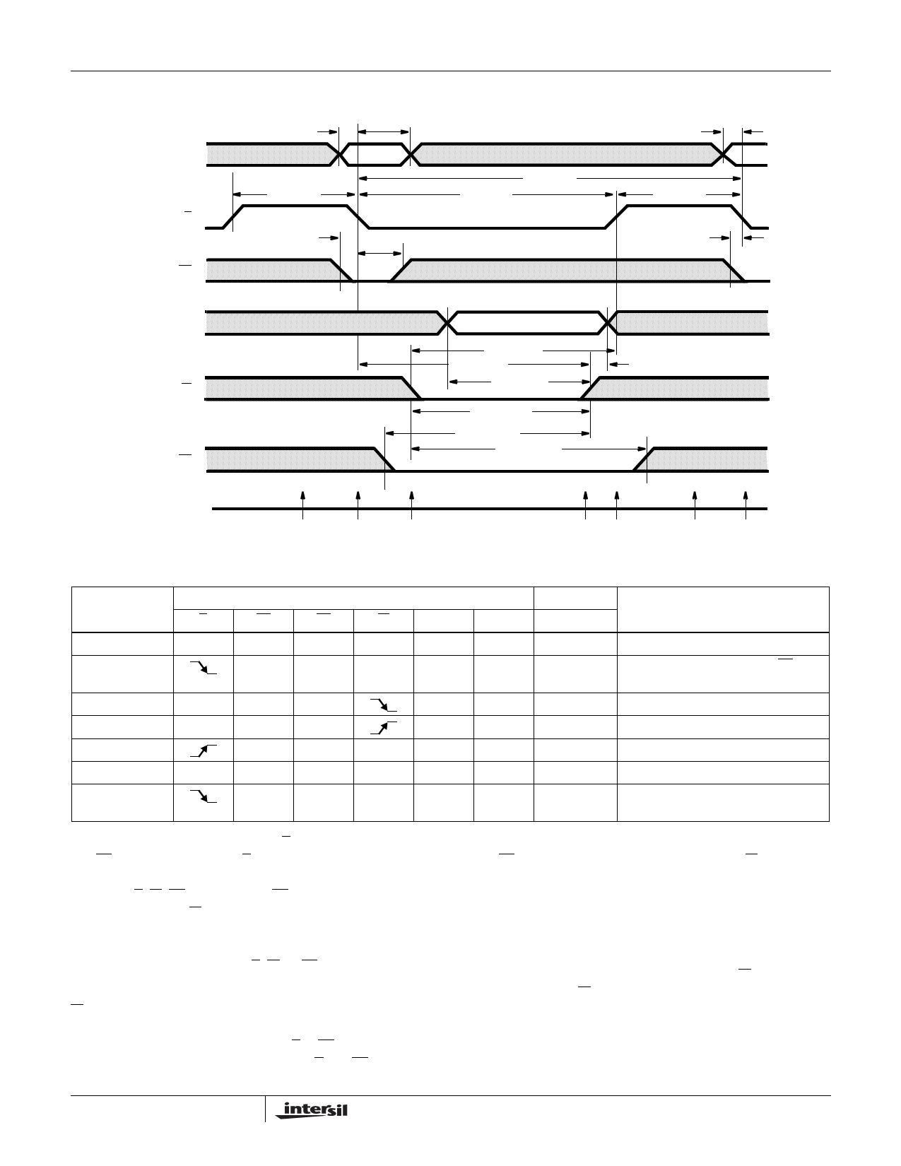
Timing Waveforms (Continued)
(8) TAVEL
A
TEHEL (7)
E
(9) TS2LEL
S2
HM-6551/883
(10)
TELAX
VALID
TELS2X
(11)
TELEL (19)
TELEH (6)
(8) TAVEL
TEHEL (7)
NEXT
(9) TS2LEL
D
W
S1
TIME
REFERENCE
DATA VALID
TWLEH (15)
TELWH (17)
TDVWH (12)
TWLWH (18)
TS1LWH (16)
TWLS1H (14)
TWHDX (13)
-1
0
1
FIGURE 2. WRITE CYCLE
23
4
5
TIME
REFERENCE
E
-1
H
0
1
L
2
L
3
4
H
5
TRUTH TABLE
INPUTS
OUTPUTS
S1
S2
W
A
D
Q
FUNCTION
H
X
X
X
X
Z
Memory Disabled
X
L
X
V
X
Z
Cycle Begins, Addresses and S2 are
Latched
L
X
X
X
Z
Write Period Begins
L
X
X
V
Z
Data In is Written
X
X
H
X
X
Z
Write is Completed
H
X
X
X
X
Z
Prepare for Next Cycle (Same as -1)
X
L
X
V
X
Z
Cycle Ends, Next Cycle Begins
(Same as 0)
In the Write Cycle the falling edge of E latches the addresses
and S2 into on-chip registers. S2 must be latched in the low
state to enable the device. The write portion of the cycle is
defined as E, W, S1 being low and S2 being latched simulta-
neously. The W line may go low at any time during the cycle
providing that the write pulse setup times (TWLEH and
TWLS1H) are met. The write portion of the cycle is terminated
on the first rising edge of either E, W, or S1.
If a series of consecutive write cycles are to be executed, the
W line may be held low until all desired locations have been
written. If this method is used, data setup and hold times must
be referenced to the first rising edge of E or S1. By positioning
the write pulse at different times within the E and S1 low time
(TELEH), various types of write cycles may be performed. If
the S1 low time (TS1LS1H) is greater than the W pulse, plus
an output enable time (TS1LQX), a combination read-write
cycle is executed. Data may be modified an indefinite number
of times during any write cycle (TELEH).
The HM-6551/883 may be used on a common I/O bus struc-
ture by tying the input and output pins together. The multiplex-
ing is accomplished internally by the W line. In the write cycle,
when W goes low, the output buffers are forced to a high
impedance state. One output disable time delay (TWLQZ)
must be allowed before applying input data to the bus.
6-107
Share Link: 