BS616UV1010 View Datasheet(PDF) - Brilliance Semiconductor
Part Name
Description
View to exact match
BS616UV1010 Datasheet PDF : 11 Pages
| |||
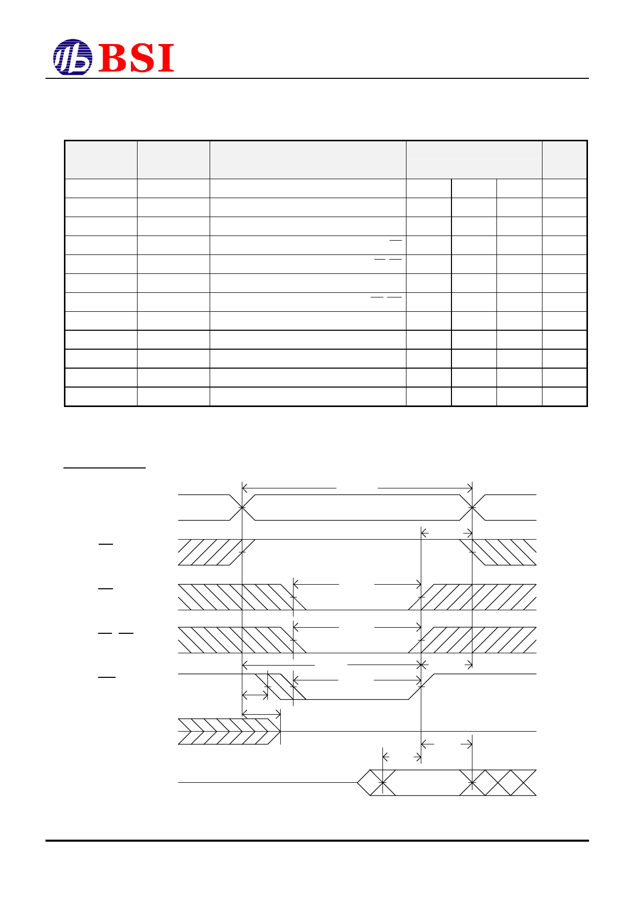
n AC ELECTRICAL CHARACTERISTICS (TA = -40OC to +85OC)
WRITE CYCLE
BS616UV1010
JEDEC
PARAMETER
NAME
tAVAX
tAVWL
tAVWH
tELWH
tBLWH
tWLWH
tWHAX
tWLQZ
tDVWH
tWHDX
tGHQZ
tWHQX
PARANETER
NAME
DESCRIPTION
tWC
tAS
tAW
tCW
tBW
tWP
tWR
tWHZ
tDW
tDH
tOHZ
tOW
Write Cycle Time
Address Set up Time
Address Valid to End of Write
Chip Select to End of Write
Data Byte Control to End of Write
Write Pulse Width
Write Recovery Time
Write to Output High Z
Data to Write Time Overlap
Data Hold from Write Time
Output Disable to Output in High Z
End of Write to Output Active
CYCLE TIME : 100ns
MIN.
TYP.
MAX.
100
--
--
0
--
--
100
--
--
(CE) 100
--
--
(LB, UB) 100
--
--
50
--
--
(CE, WE)
0
--
--
--
--
40
40
--
--
0
--
--
--
--
40
10
--
--
UNITS
ns
ns
ns
ns
ns
ns
ns
ns
ns
ns
ns
ns
n SWITCHING WAVEFORMS (WRITE CYCLE)
WRITE CYCLE 1 (1)
ADDRESS
OE
tWC
tWR1(3)
tCW(11)
CE
(5)
LB, UB
WE
DOUT
DIN
tAS
tOHZ(4,10)
tBW
tAW
tWP(2)
tWR2(3)
tDH
tDW
R0201-BS616UV1010
7
Revision 2.6
May.
2006
Share Link: 