AT27C2048-55JC(1998) View Datasheet(PDF) - Atmel Corporation
Part Name
Description
View to exact match
AT27C2048-55JC Datasheet PDF : 12 Pages
| |||
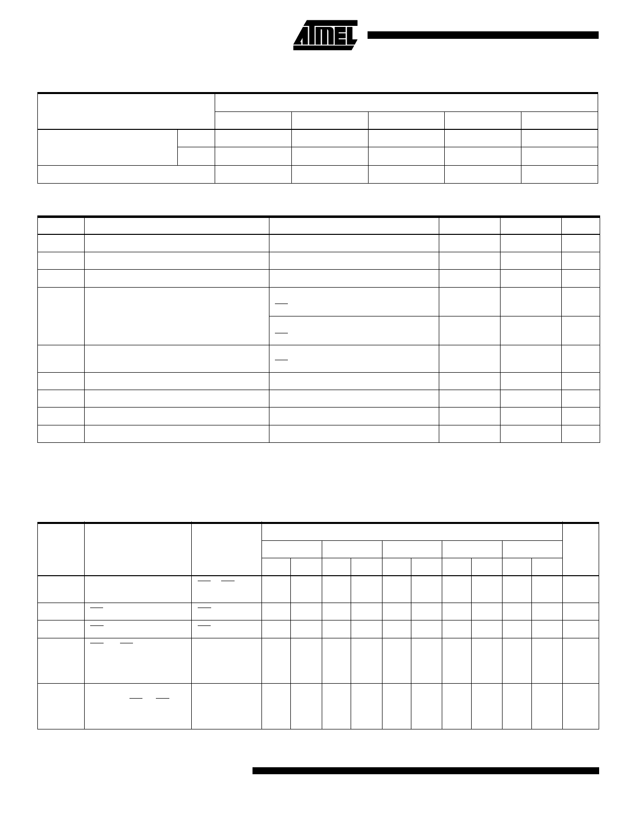
DC and Operating Characteristics for Read Operation
Symbol Parameter
Condition
Min
Max
Units
ILI
Input Load Current
VIN = 0V to VCC
±1
µA
ILO
IPP1(2)
Output Leakage Current
VPP(1) Read/Standby Current
VOUT = 0V to VCC
VPP = VCC
±5
µA
10
µA
ISB1 (CMOS)
ISB
VCC(1) Standby Current
CE = VCC ± 0.3V
ISB2 (TTL)
CE = 2.0 to VCC + 0.5V
100
µA
1
mA
ICC
VCC Active Current
f = 5 MHz, IOUT = 0 mA, CE = VIL
35
mA
VIL
Input Low Voltage
-0.6
0.8
V
VIH
Input High Voltage
2.0
VCC + 0.5
V
VOL
Output Low Voltage
IOL = 2.1 mA
0.4
V
VOH
Notes:
Output High Voltage
IOH = -400 µA
2.4
V
1. VCC must be applied simultaneously or before VPP, and removed simultaneously or after VPP.
2. VPP may be connected directly to VCC, except during programming. The supply current would then be the sum of ICC and IPP.
AC Characteristics for Read Operation
-55
-70
Symbol Parameter
Condition
Min Max Min Max
tACC(3)
tCE(2)
tOE(2)(3)
tDF(4)(5)
Address to
Output Delay
CE = OE
= VIL
CE to Output Delay
OE = VIL
OE to Output Delay
CE = VIL
OE or CE High to Output Float,
whichever occurred first
55
70
55
70
20
30
20
20
tOH(4)
Note:
Output Hold from Address, CE or OE,
whichever occurred first
7
7
2, 3, 4, 5. See the AC Waveforms for Read Operation diagram.
AT27C2048
-90
Min Max
90
90
35
20
0
-12
Min Max
120
120
40
30
0
-15
Min Max
150
150
50
35
0
Units
ns
ns
ns
ns
ns
4
AT27C2048
Share Link: 