MSK642 View Datasheet(PDF) - M.S. Kennedy
Part Name
Description
View to exact match
MSK642 Datasheet PDF : 6 Pages
| |||
APPLICATION NOTES
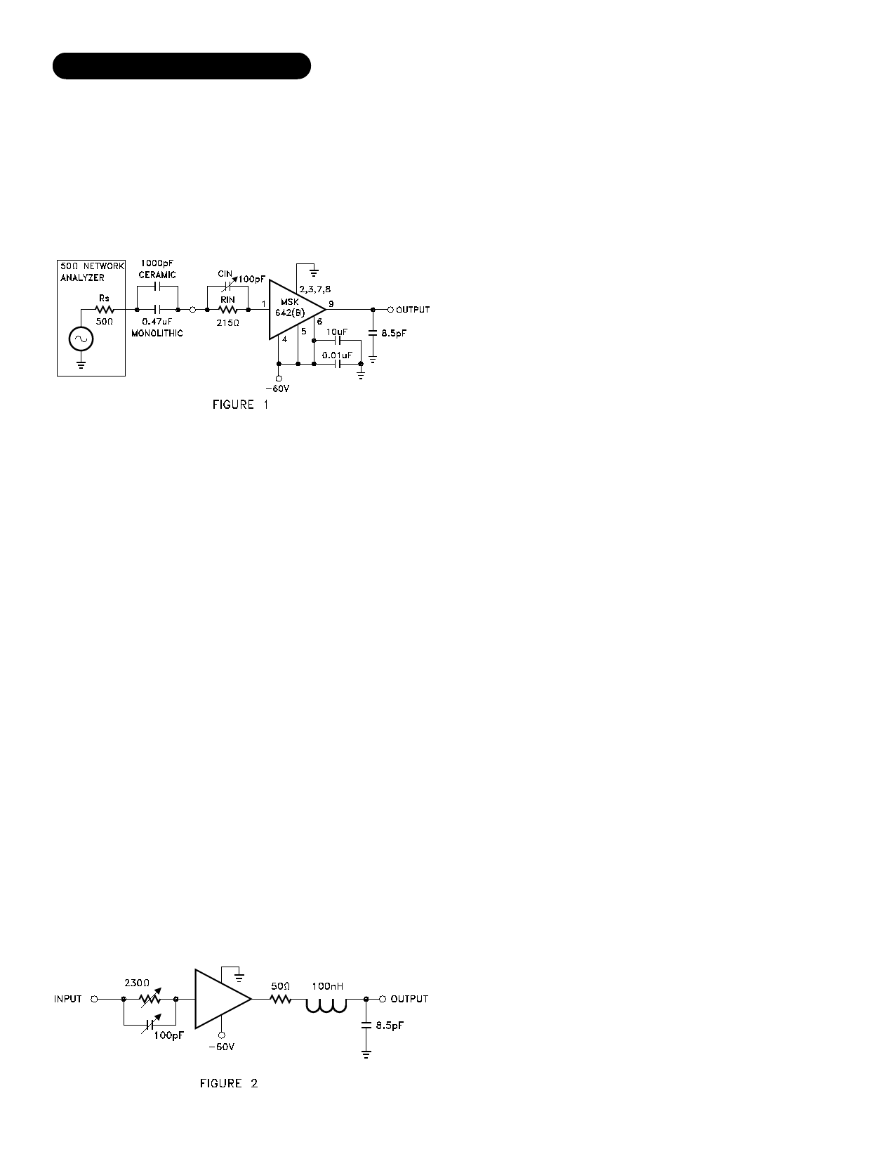
TYPICAL TEST CIRCUIT
The signal source in Figure 1 can be either a fast pulse gen-
erator or a network analyzer as long as the output impedance is
50 ohms. The DC level of the input should be -1.55V and all
cables should be kept as short as possible. Since total load
capacitance should be kept below 8.5pF, a FET probe should
be used on the ouput.
USING THE MSK 642
The output of the amplifier is biased at one half of the power
supply voltage. An output voltage swing of ±25 volts is typi-
cal with a power supply voltage of -60 volts. With an 8.5pF
capacitive load, transistion times are in the 2.5nS range. If a
spark gap current limiting resistor is used on the output of the
amplifier and the transistion times are degraded, a peaking coil
may be used to preserve system performance. The optimum
value for this coil will be in the range of 100 to 200nH and can
best be determined by trial and error. The output of the MSK
642 is not short circuit protected, therefore, purely resistive
loads should be no less than 600 ohms at any time to avoid
damaging the output.
OPERATION CONSIDERATIONS
The input of the MSK 642 rests at a -1.55VDC level with the
input terminal open. In this state, the output rests at one half
of the power supply voltage. When connecting a pulse genera-
tor to the input of the amplifier, the DC level should be offset
so that the signal is centered around -1.55V. During character-
ization, the input should be coupled to the MSK 642 through a
parallel combination of a variable resistor and variable capacitor
peaking circuit. Optimum values for the peaking circuit can be
determined experimentally. The optimum value of load capaci-
tance is 8.5pF. Viewing the output with a normal oscilloscope
probe would seriously degrade performance. A FET probe fit-
ted with a 100:1 voltage divider will add only approximately
1.5pF of capacitance to the load and is highly recommended.
An experimental circuit along with recommended values can be
found in Figure 2.
OUTPUT ISSUES
The output of the MSK 642 is a pair of bipolar emitter follow-
ers configured in a complimentary push pull configuration. This
configuration eliminates the need for a pull up load resistor and
makes the amplifier less susceptible to load capacitance varia-
tions. Connecting a wire or cable from the output of the ampli-
fier to the CRT grid can create a resonant circuit which can
cause unwanted oscillations or overshoot at its resonant fre-
quency. A damping resistor in series with the lead inductance
will alleviate this condition. The optimum value of this resistor
can be determined using the following formula:
R = 2* √L/C
This resistor also doubles as an arcing protector. In the bread-
boarding stage, the value of this resistor should be determined
experimentally. Resistance in the range of 50 to 100 ohms is
usually sufficient. If a quick, simple peaking network is de-
sired, a 300 ohm cable terminated by a capacitor will act like an
inductor in the frequency range involved.
TRANSIMPEDANCE AMPLIFICATION
Transimpedance amplifiers relate input current to output volt-
age. The MSK 642 contains an internal 3KΩ feedback resistor.
This resistor converts input current to output voltage in the
following manner (See Figure 1):
±1.43V (referenced to -1.55Vdc) across the 215Ω input
resistor results in an input current of ±6.65mA. This current
flows through the 3KΩ feedback resistor and results approxi-
mately in a ±20V swing at the output. The actual voltage gain
of the typical MSK 642 circuit may be slightly less due to tran-
sistor losses. The following formula approximates voltage gain
including potential losses:
Voltage Gain (V/V) = 3KΩ/(Rin + L)
L ≈ 25Ω
HEAT SINKING
The MSK 642 requires heat sinking in most applications. The
following formula may be applied to determine if a heat sink is
necessary and what size and type to use.
Rθsa = ((Tj-Ta)/Pd ) - (Rθjc) - (Rθcs)
WHERE
Tj = Junction Temperature
Pd = Total power dissipation
Rθjc = Junction to case thermal resistance
Rθcs = Case to heat sink thermal resistance
Rθsa = Heat sink to ambient thermal resistance
Tc = Case temperature
Ta = Ambient temperature
Ts = Sink temperature
EXAMPLE
Tj = 150°C
Ta = 100°C
Pd = 1.5W
Rθjc = 27°C/W
Rθcs = 0.15°C/W
Solving the above equation for Rθsa (heat sink thermal conduc-
tivity) shows that the heat sink for this application must have a
thermal resistance of no more than 6.0°C/W to maintain a junc-
tion temperature of no more than 150°C.
3
Rev. E 10/05
Share Link: 