MSK642(2000) View Datasheet(PDF) - M.S. Kennedy
Part Name
Description
View to exact match
MSK642 Datasheet PDF : 6 Pages
| |||
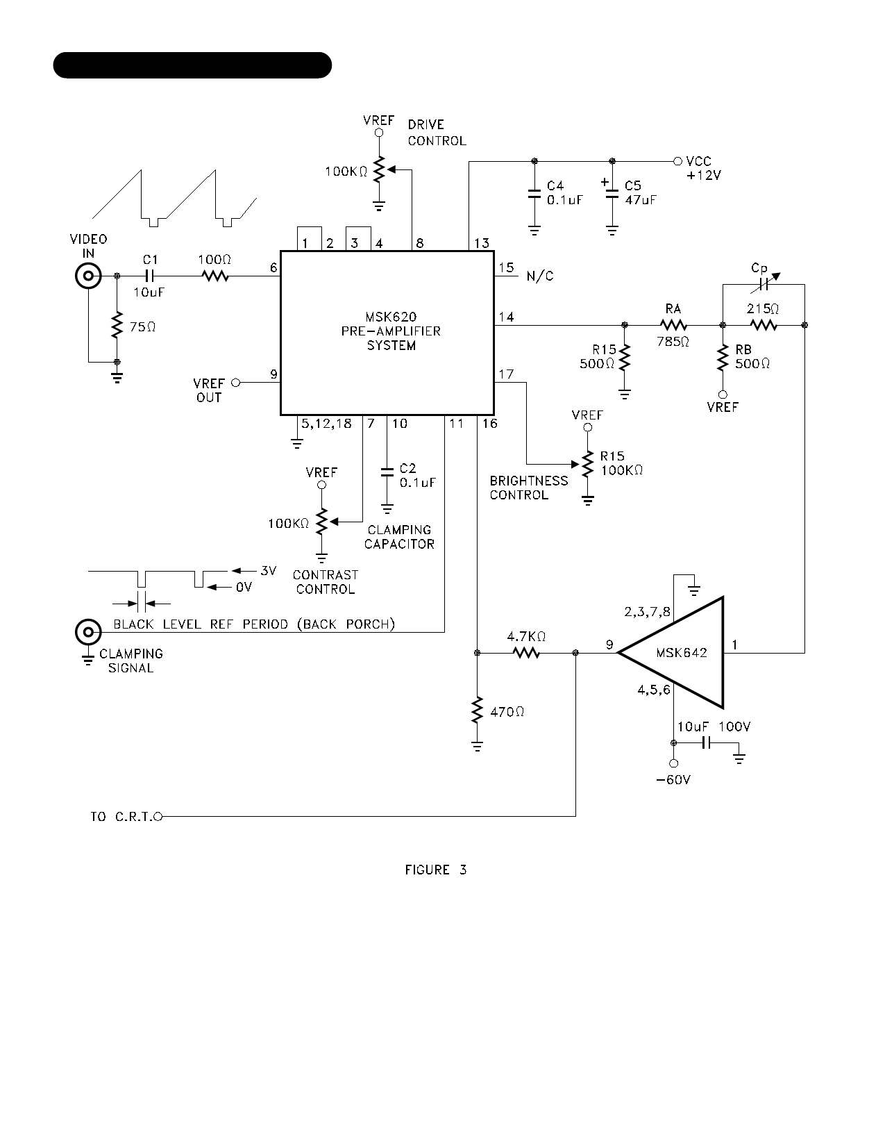
COMPLETE VIDEO SYSTEM
Figure 3 above illustrates how an MSK 620 and MSK 642 can be used to build a compete video system for high voltage grid
drive. RA and RB act as a level shift stage to match the +3.9Vdc level at the output of the MSK 620 with the -1.55Vdc level at
the input of the MSK 642. The output of the MSK 642 is sampled and fed back to the MSK 620. This scheme provides black level
control superior to sampling the signal at pin 14 of the MSK 620. The general rule of thumb for transition times for a video driver
is that rising and falling edges should be no more than one third the pixel time of the monitor. To improve rise and fall time in the
system, the peaking capacitor Cp was added across the input resistor of the MSK 642. At high frequencies Cp increases the gain
of the amplifier there by causing peaking. Cp should be a variable capacitor so that the response of the amplifier can be fine tuned
for minimum transition time with minimum ringing.
5
Rev. B 8/00
Share Link: 