MSK601 View Datasheet(PDF) - M.S. Kennedy
Part Name
Description
View to exact match
MSK601 Datasheet PDF : 4 Pages
| |||
APPLICATION NOTES
FEED FORWARD TOPOLOGY
The MSK 601 employs a circuit topology known as "feed
forward". This inverting configuration allows the user to real-
ize the excellent D.C. input characteristics of a differential am-
plifier without losing system bandwidth. The incoming sig-
nal is split at the input into its A.C. and D.C. component. The
D.C. component is allowed to run through the differential
amplifier where any common mode noise is rejected. The
A.C. component is "fed forward" to the output section through
a very high speed linear amplifier where it is mixed back to-
gether with the D.C. component. The result is an amplifier
with most of the benefits of a differential amplifier without the
loss in system bandwidth.
HIGH VOLTAGE SUPPLIES
The positive and negative high voltage supplies on the MSK
601 can be adjusted to reduce power dissipation. The out-
put of the MSK 601 will typically swing to within 8V of
either high voltage power supply rail. Therefore, if the sys-
tem in question only needs the output of the amplifier to swing
±40V peak, the power supply rails could be set to ±50V.
For best performance, the minimum value of ±VHV should be
±50VDC. Unbalanced power supply rails are also allowed as
long as one or the other is not decreased to below 30V or
above 150V. The high voltage and low voltage power sup-
plies should be decoupled as shown in Figure 1.
TRANSITION TIMES
Transition time optimization of the MSK 601 follows the
same basic rules as most any other amplifier. Best transition
times will be realized with minumum load capacitance, mini-
mum external feedback resistance and lowest circuit gain.
Transition times will degrade if the output is driven too close
to either supply rail. Feedback and input resistor values will
affect transition time as well. See Figure 1 and Table 1 for
recommended component values.
VOLTAGE
GAIN
-10V/V
-20V/V
-50V/V
-RIN
RF
1KΩ
499Ω
402Ω
10KΩ
10KΩ
20KΩ
Table 1
CF
0.5-5pF
N/A
N/A
INTERNAL COMPENSATION
Since the MSK 601 is a high voltage amplifier, it is com-
monly used in circuits employing large gains. Therefore, the
internal compensation was chosen for gains of -5V/V or greater.
In circuits running at gains of less than -5V/V, the user can
further compensate the device by adding compensation net-
works at the input or feedback node. Pin 1 (comp) should be
bypassed with a 0.1uF ceramic capacitor to +VHV for all ap-
plications.
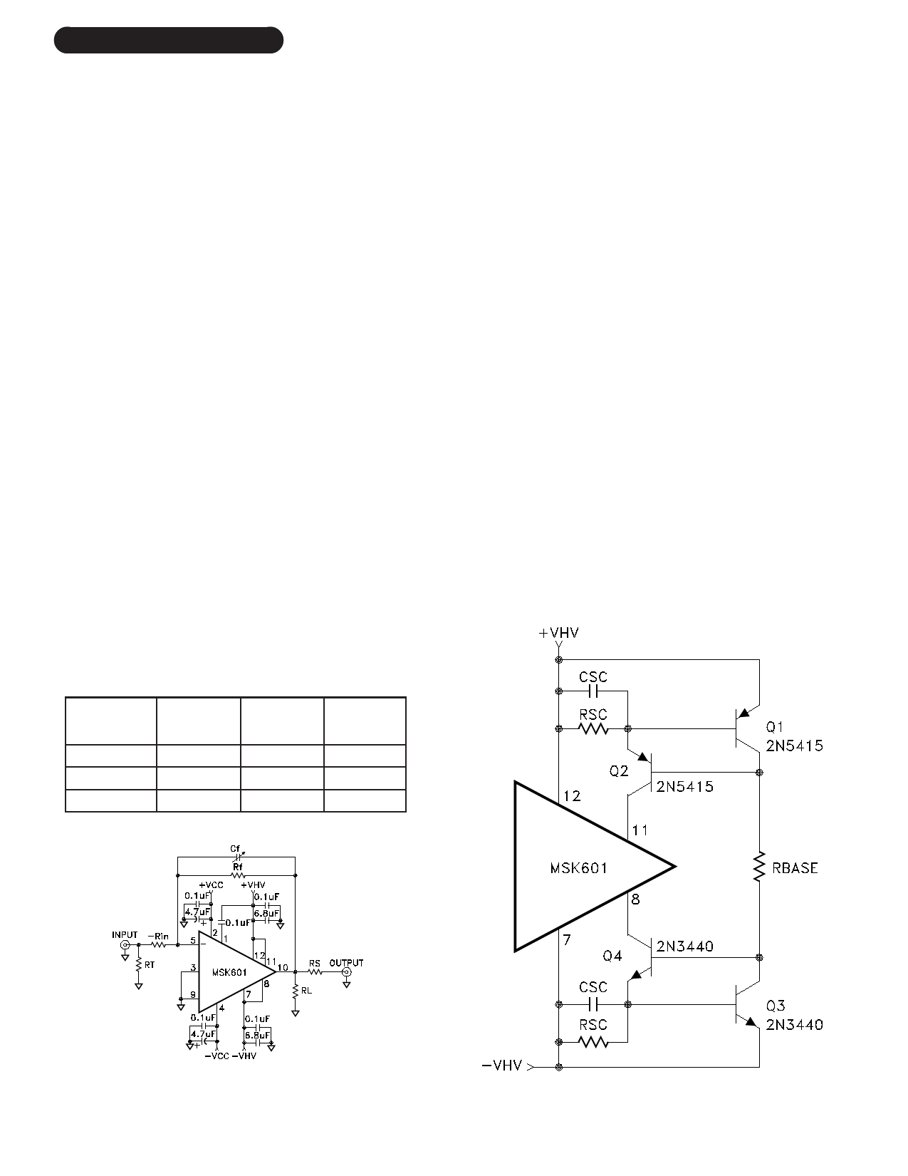
CURRENT LIMIT
Figure 2 is the recommended active short circuit protection
scheme for the MSK 601. The following formula may be
used for setting current limit:
Current Limit ≈ 0.6V / Rsc
RBASE must be selected based on the value of ±VHV as fol-
lows:
RBASE = ((+VHV - (-VHV)) - 1.2V) / 4mA
This formula guarantees that Q2 and Q4 will always have
sufficient base current to be in operation. This circuit can be
made tolerant of high frequency output current spikes with
the addition of CSC. The corresponding time constant would
be:
T = (RSC) (CSC)
A common value for CSC is approximately 1000pF. If current
limit is unnecessary, short pin 7 to pin 8 and pin 11 to pin 12
as shown in Figure 1.
Figure 1
Figure 2
3
Rev. B 9/11
Share Link: 