EL4501CS View Datasheet(PDF) - Elantec -> Intersil
Part Name
Description
View to exact match
EL4501CS Datasheet PDF : 10 Pages
| |||

EL4501C - Preliminary
Video Front End
Absolute Maximum Ratings (TA = 25°C)
Values beyond absolute maximum ratings can cause the device to be pre-
maturely damaged. Absolute maximum ratings are stress ratings only and
functional device operation is not implied.
Supply Voltage (VS to GND)
+6V
Input Voltage
GND - 0.3V, VS +0.3V
Storage Temperature Range
Ambient Operating Temperature
Operating Junction Temperature
Power Dissipation
-65°C to +150°C
-40°C to +85°C
125°C
See Curves
Important Note:
All parameters having Min/Max specifications are guaranteed. Typ values are for information purposes only. Unless otherwise noted, all tests are at the
specified temperature and are pulsed tests, therefore: TJ = TC = TA.
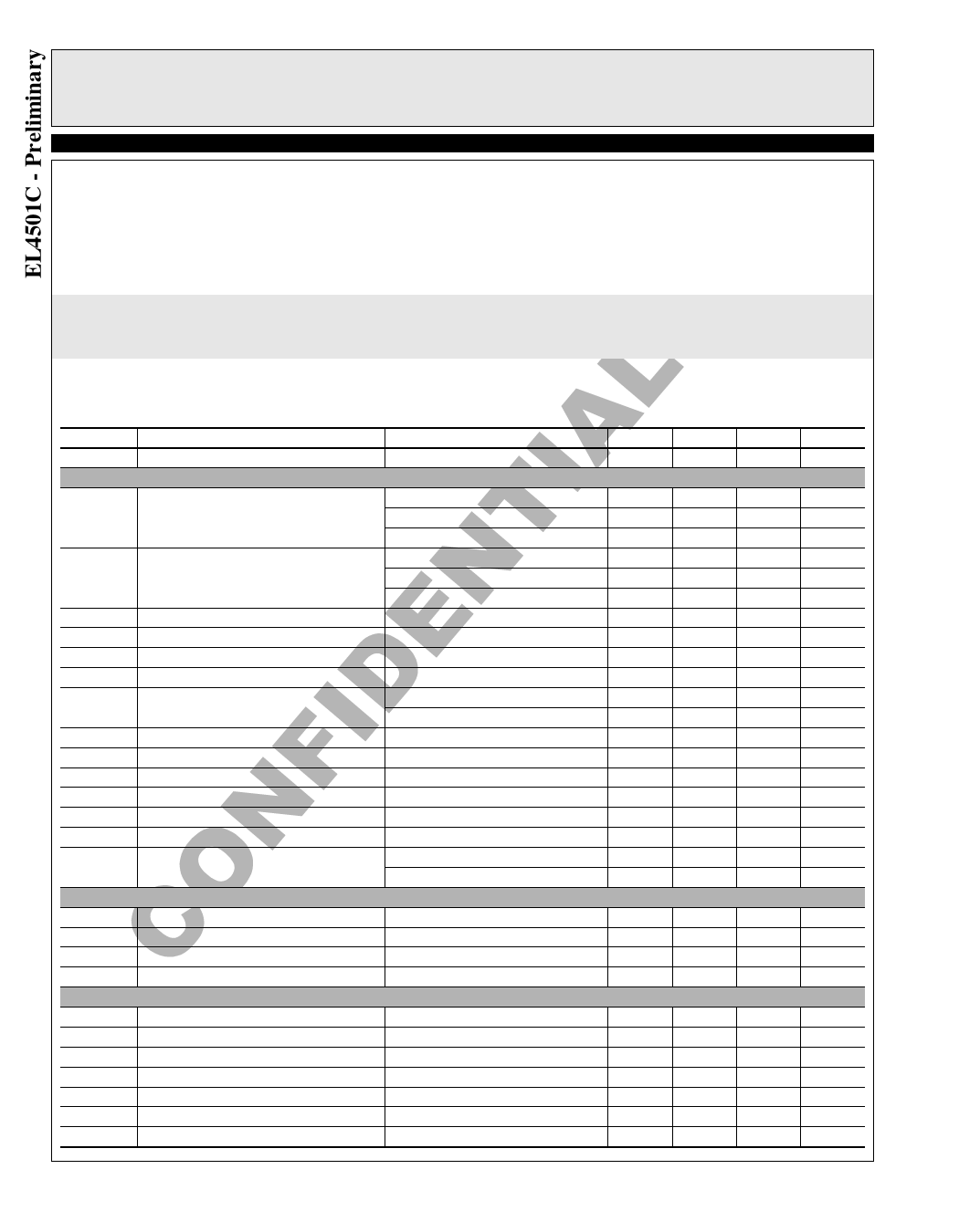
Electrical Characteristics
VS = +5V, GND = 0V, TA = 25°C, Input Video = 1VP-P unless otherwise specified.
Parameter
Description
Conditions
Min
Typ
Max
Unit
IS
Supply Current
No Load, VIN = 0V
20
mA
Video Amplifier Section
VOP
Positive Output Voltage Swing
RL = 150Ω to VS/2
RL = 150Ω to GND
4.70
4.85
V
4.20
4.60
V
VON
Negative Output Voltage Swing
+IOUT
-IOUT
dG
dP
BW
Positive Output Current
Negative Output Current
Differential Gain Error [1]
Differential Phase Error [1]
Bandwidth
RL = 1k to VS/2
4.95
4.97
V
RL = 150Ω to VS/2
0.15
0.30
V
RL = 150Ω to GND
0
V
RL = 1k to VS/2
0.03
0.05
V
RL = 10Ω to VS/2
60
80
120
mA
RL = 10Ω to VS/2
-50
-60
-80
mA
Standard NTSC test, AV = 2, RL = 150Ω
0.1
%
Standard NTSC test, AV = 2, RL = 150Ω
0.1
°
-3dB, G = 1, RL = 10kΩ to GND
100
MHz
-3dB, G = 1, RL = 150Ω to GND
60
MHz
BW1
Bandwidth
+/-0.1dB, G = 2, RL = 150Ω to GND
8
MHz
SR
Slew Rate
25% to 75%, 3.5VP-P, RL = 150Ω
150
200
V/µ s
VRL
Ref Level Range
ts
Settling Time
RIN
Input Resistance (VIDEO_IN)
to 0.1%, VIN = 0V to 3V
0
3.5
V
35
ns
90
115
140
kΩ
CIN
Input Capacitance (VIDEO_IN)
1.5
pF
AVOL
Open Loop Voltage Gain
RL = no load, VOUT = 0.5V to 3V
54
65
dB
RL = 150Ω to GND, VOUT = 0.5V to 3V
40
50
dB
DC Restore Section
CMIR
Common Mode Input Range (REF_IN)
CMRR ≥ TBD dB
0
3.5
V
VOS
TCVOS
Input Offset Voltage
Input Offset Voltage Temperature Coefficient
DC restored
-20
+20
mV
10
µ V/°C
IB
Input Bias Current (REF_IN)
VCM = 0V to 3.5V
1
100
nA
Data Slicer Section
IIH
Input High Current (DS_MODE & DS_ENAB) VIH = 5V
4
6
µA
IIL
Input Low Current (DS_MODE & DS_ENAB) VIL = 0V
1
100
nA
VIH
Input High Voltage (DS_MODE & DS_ENAB)
4.5
V
VIL
Input Low Voltage (DS_MODE & DS_ENAB)
0.5
V
VOH
Output High Voltage (DS_OUT)
IOUT = -1mA
4.75
4.9
V
VOL
IOUT
Output Low Voltage (DS_OUT)
Short Circuit Current (DS_OUT)
IOUT = 1mA
RL = 10Ω to 2.5V
0.1
0.25
V
15
20
mA
2