C9001 View Datasheet(PDF) - Hamamatsu Photonics
Part Name
Description
View to exact match
C9001 Datasheet PDF : 2 Pages
| |||
Driver circuit for CMOS linear image sensor C9001
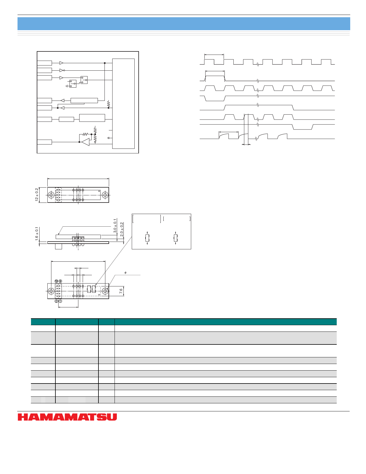
I Block diagram
CLK
START
SW2: EXTERNAL/INTERNAL GAIN CHANGE
GAIN
+5 Vcc
S8377/S8378
P-CLK
P-ST
Vg
TRIG
EOS
+5 Vcc
VIDEO
SW1: INTERNAL GAIN CHANGE
GATE CIRCUIT
Vcc
eos
FILTER
CLAMP VOLTAGE
GENERATOR
Vcc
Vcc
-
+
Vclamp
Vdd
Vss
Video
I Dimensional outline (unit: mm)
50 ± 0.2
41
KACCC0174EA
I Timing chart
DUTY RATIO 50 %
CLK
1 CLK WIDTH
START
P-CLK *
P-ST *
GATE *
TRIG
EOS
VIDEO
1 CLK WIDTH
* INTERNAL SIGNAL
APPROX. 100 ns
KACCC0175EA
58
CMOS LINEAR IMAGE SENSOR
S8377/S8378 SERIES
(SOLD SEPARATELY)
SENSOR GAIN SELECTION SWITCH
CIRCUIT/EXTERNAL
SWITCH
CIRCUIT SWITCH
CIRCUIT SWITCH
SELECTION
SENSOR GAIN High
S2
S1
44
2.54
2.54
2.54
EXTERNAL SELECTION SENSOR GAIN Low
SET UP AT
SHIPMENT
S2: CIRCUIT SWITCH
SELECTION
S1: SENSOR GAIN Low
(2 ×) 2.5 ± 0.1
S2
S1
16.1 ± 0.1
KACCA0115EA
I Pin assignment of I/O connector [Connector: LY20-10P-DTI-P1 (made by JAE) ] *3
Pin No. Terminal name I/O
Description
➀
CLK
I Sensor scan synchronization signal. The sensor is scanned in synchronization with this signal.
➁
START
I
Sensor scan start signal. The pulse interval of these start signals determines the sensor integration
time.
➂
GAIN
I
Sensor gain setting. Low gain is selected at High level, and high gain at Low level. (External
gain setting is enabled with S2.)
➃
EOS
O Sensor end-of-scan signal. Negative logic
➄
TRIG
O A/D conversion timing signal. The number of output pulses is equal to the number of pixels.
➅
GND
Circuit ground
➆
Vcc
I +5 V power supply line
➇
GND
Circuit ground
➈
VIDEO
O Video output signal. Positive polarity
➉
A.GND
Video signal ground
*3: A mating connector is supplied with C9001 along with toa cable (30 cm, preassembled).
Information furnished by HAMAMATSU is believed to be reliable. However, no responsibility is assumed for possible inaccuracies or omissions.
Specifications are subject to change without notice. No patent rights are granted to any of the circuits described herein. ©2002 Hamamatsu Photonics K.K.
HAMAMATSU PHOTONICS K.K., Solid State Division
1126-1 Ichino-cho, Hamamatsu City, 435-8558 Japan, Telephone: (81) 053-434-3311, Fax: (81) 053-434-5184, http://www.hamamatsu.com
U.S.A.: Hamamatsu Corporation: 360 Foothill Road, P.O.Box 6910, Bridgewater, N.J. 08807-0910, U.S.A., Telephone: (1) 908-231-0960, Fax: (1) 908-231-1218
Germany: Hamamatsu Photonics Deutschland GmbH: Arzbergerstr. 10, D-82211 Herrsching am Ammersee, Germany, Telephone: (49) 08152-3750, Fax: (49) 08152-2658
France: Hamamatsu Photonics France S.A.R.L.: 8, Rue du Saule Trapu, Parc du Moulin de Massy, 91882 Massy Cedex, France, Telephone: 33-(1) 69 53 71 00, Fax: 33-(1) 69 53 71 10
United Kingdom: Hamamatsu Photonics UK Limited: 2 Howard Court, 10 Tewin Road, Welwyn Garden City, Hertfordshire AL7 1BW, United Kingdom, Telephone: (44) 1707-294888, Fax: (44) 1707-325777
North Europe: Hamamatsu Photonics Norden AB: Smidesvägen 12, SE-171 41 Solna, Sweden, Telephone: (46) 8-509-031-00, Fax: (46) 8-509-031-01
Italy: Hamamatsu Photonics Italia S.R.L.: Strada della Moia, 1/E, 20020 Arese, (Milano), Italy, Telephone: (39) 02-935-81-733, Fax: (39) 02-935-81-741
Cat. No. KACC1079E01
2
Jul. 2002 DN
Share Link: 