MX10C8052 View Datasheet(PDF) - Macronix International
Part Name
Description
View to exact match
MX10C8052 Datasheet PDF : 14 Pages
| |||
MX10C805X
External clock drive XTAL
SYMBOL
PARAMETER
fCLK
tCLCL
tCHCX
tCLCX
tCLCH
tCHCL
tCY
clock frequency
clock period
HIGH time
LOW time
RISE time
FALL time
cycle time (tCY = 12 tCK)
VARIABLE CLOCK
MIN
MAX
1.2
16 (tbf.)
63
833
20
tCK-tCLCX
20
tCK-tCHCX
-
20
-
20
0.75
10
UNIT
MHz
ns
ns
ns
ns
ns
ms
SERIAL PORT CHARACTERISTICS
Serial Port Timing : Shift Register Mode
VDD = 5V±10%; VSS = 0V; Tamb=0°C; Load Capacitance = 80 pF
SYMBOL
PARAMETER
tXLXL
tQVXH
tXHQX
tXHDX
tXHDV
Serial Port clock cycle time
Output data setup to clock rising edge
Output data hold after clock rising edge
Input data hold after clock rising edge
Clock rising edge to input data valid
33 MHz OSCILLATOR
MIN
MAX
360
-
167
-
5
-
0
-
-
167
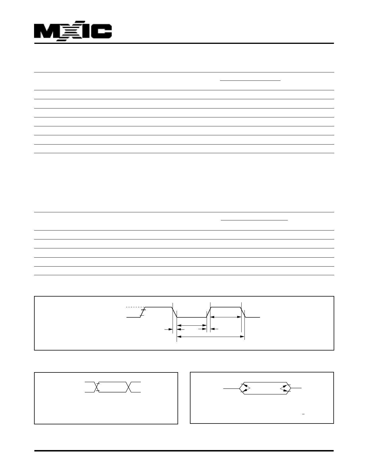
EXTERNAL CLOCK DRIVE WAVEFORM
VCC-0.5
0.45V
0.7 VCC
0.2 VCC-0.1
TCHCL
TCLCX
TCHCX
TCLCH
TCLCL
UNIT
ns
ns
ns
ns
ns
AC TESTING INPUT, OUTPUT WAVEFORMS
VCC-0.5
0.45V
0.2 VCC+0.9
0.2 VCC-0.1
AC Inputs during testing are driven at VCC-0.5V for a
Logic "1" 0.45V for a Logic "0". Timing measurements
are made at VIH min for a Logic "1" and VIL max for a
Logic "0".
FLOAT WAVEFORM
VLOAD+0.1V
VLOAD
VLOAD-0.1V
TIMING REFERENCE
POINTS
VOH-0.1V
VOL+0.1V
For timing purposes a port pin is no longer floating when a 100 mV
change from load voltage occurs, and begins to float when a 100mV
change form the loaded VOH/VOL level occurs. IOL/IOH = + 20 mA
P/N:PM0591
REV. 0.3, APR. 09, 1999
10
Share Link: 