PD45128168G5-A10-9JF View Datasheet(PDF) - Elpida Memory, Inc
Part Name
Description
View to exact match
PD45128168G5-A10-9JF Datasheet PDF : 92 Pages
| |||
µPD45128441, 45128841, 45128163
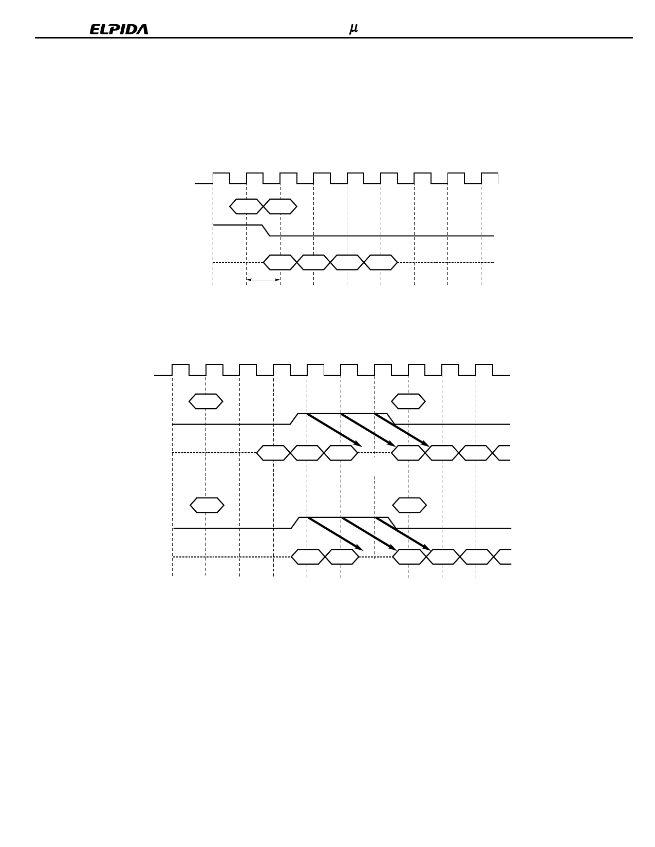
11.4 Read to Write Command Interval
During a read cycle, READ can be interrupted by WRITE.
The Read and Write command interval is 1 cycle minimum. There is a restriction to avoid data conflict. The Data
bus must be Hi-Z using DQM before WRITE.
Burst length = 4
T0
T1
T2
T3
T4
T5
T6
T7
T8
CLK
Command
DQM
DQ
READ WRITE
Hi-Z
D1
D2
D3
D4
1cycle
READ can be interrupted by WRITE. DQM must be High at least 3 clocks prior to the Write command.
Burst length = 8
T0
T1
T2
T3
T4
T5
T6
T7
T8
T9
CLK
/CAS latency = 2
Command
READ
WRITE
DQM
DQ
/CAS latency = 3
Command
DQM
READ
Q1
Q2
Q3
D1
D2
D3
Hi-Z is
necessary
WRITE
DQ
Q1
Q2
D1
D2
D3
Hi-Z is
necessary
30
Data Sheet E0031N30
Share Link: 